Heterogeneous IC packaging is here. It is already in production, and increasingly more customers are developing and qualifying their products at Amkor and in other outsourced semiconductor assembly and test (OSAT) suppliers and foundry providers.
The rationale for this surge into new multi-die embodiments has been well documented and discussed. In the final analysis, more of the system content is moving into the package itself, with benefits in performance, cost, and time-to-market (TTM). Total silicon costs can be lower due to better yields for smaller chiplets. Heterogeneous packaging also provides the opportunity to use a mixture of silicon process nodes to further optimize the cost of the silicon. While heterogeneous IC packages are more expensive, the positive tradeoffs/benefits are lower total silicon cost and positive TTM benefits. Moving to a heterogeneous approach requires an infrastructure to be established in design, IC and package fabrication, and test.
IC packaging options to support chiplets and the heterogeneous constructions have propagated as each OSAT and foundry offers its own version. As a result, the terminology has become quite confusing. Thankfully, these package constructions are much simpler than the terminology that is now present in the industry. Multi-die products must be integrated into one functional unit and that is done on either classical IC package substrates or by using higher-density integration approaches, namely wafer-scale multi-die modules, ultra-fine line integrations, or both. The module is then attached to the IC package substrate.
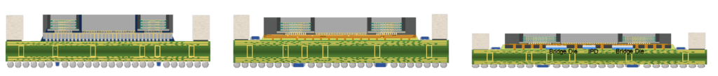
The first option is typified by the long-standing multichip module (MCM), which has been in production for decades, with modern designs trending to higher silicon and passive density on the substrate. The second option for higher-density integration approaches is to create modules that integrate the die or chiplets, which needs ultra-fine-line routing for die-die interfaces. Today, these are (A) modules based on silicon interposers – 2.5D through silicon vias (TSVs), (B) modules based on high-density fan-out (HDFO) multi-layer redistribution layer (RDL) approaches, or (C) modules with bridges as shown in Figure 1.
Heterogeneous IC Packaging Designs
Modules based on HDFO interposers have been internally qualified, are customer products, and are in qualification. The quantity of different devices using HDFO interposers in the market is still limited as the transition to chiplets has just been initiated. However, the market is changing and most advanced-packaging customers that are already producing higher-end monolithic or MCM devices are either actively qualifying HDFO interposers or inquiring, with the intent to start development.
In the initial planning phase of a product that incorporates an HDFO module, it is important to understand that each device is likely to be considered “custom.” While the qualification envelope may encompass the overall module and package size under consideration, each device has unique challenges. For this reason, almost every new device has iterations of test vehicles. As more test vehicles (TVs) are successfully completed and more of the possible design space variety is qualified, moving directly to product qualification will be likely, but for the moment, a TV is highly advised.
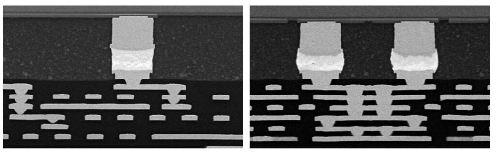
The first typically used TV is a daisy-chain die or at least bumped dummy die to allow for the discovery of any unique characteristics of the multi-die layout in the module. Assessing the interposer carrier and overmolding wafer-level warpage is a good example. Mechanical simulations can be used to estimate warpage but although simulating full wafer-level warpage is possible, it is also very sensitive to things like metal density in the RDLs. It is always possible to establish trends in simulation, but the final assessment needs to be established with actual TVs. Since TVs can be internally fabricated relatively quickly, a simulation can be calibrated to real-world data quickly so that the trends can be understood when changing different elements in the model/device. By building the mechanical or daisy chain TV, data can be gathered quickly to understand where any engineering efforts will need to be focused. This has been repeated over many TV constructions to date and is a well-known process development path in Amkor. Figures 2a and b show typical TV approaches.

The second TV can be another daisy-chain device or have some minimal functionality or chip-package interaction (CPI) test structures in the die(s). Even though the dies are likely not fully functional, the design itself will either be similar to the functional design or can actually be the functional design. The design of the interposer RDLs typically starts before the first TV, since the chiplet interfaces are still customer-specific between dies. Finding the best routing strategy requires close collaboration between the customer and fabricator, as the design rules are continuously improving. Depending on when the product is targeted for production, more advanced design rules that are still in development may be available, which would enable routing that initial design rules would not allow. Every customer has their own preference for the design process flow. Amkor tries to accommodate all preferences, ranging from receiving only the finished graphic data stream (GDS) of the interposer to managing the entire design process.
The HDFO interposer design process typically begins with a starter database provided by the Amkor design team in either Cadence (SIP/MCM file) or Siemens Expedition. The starter database is not required but automatically initiates with the standard design rules and necessary settings to interface with a Calibre design rule checking (DRC) implementation, thus saving time. Amkor can also help to set up these parameters in whichever electronic design automation (EDA) tool is used. The Calibre DRC rule deck can be run either by Amkor or the customer since it runs directly on the GDS that is exported from the EDA tool.
For larger, more complicated interposers, the design process can range from 4 to 12 weeks. The EDA tools have improved significantly in the years since Amkor introduced its SWIFT® HDFO technology. The dynamic fill step can take significantly longer to process than most designers are accustomed to, so anticipating the added time in a production schedule is important at the outset. This is due to the extremely high number of pins, traces, and shapes present in the design. Degassing or thieving, depending on which is desired, is typically the last operation performed before the design is released. Amkor has developed approaches that can reduce the time degassing or thieving takes, but for large designs, this can be a multi-day activity.
Once the design is complete, it is released to the HDFO line to start the RDL build-up process. While the second TV’s HDFO interposer is being fabricated, data will typically be collected on the first TV. This allows planning for any required design of experiments (DOEs) on the second TV. Not every device requires DOEs, but this is a crucial step so that any required improvements can be flagged and either fixed or mitigated before the start of the assembly of the second TV.
The second test vehicle is typically used for package qualifications. HDFO modules have proven to be incredibly robust, passing moisture sensitivity testing level 1 (MSL1) and Temperature Cycle, Condition C (TCC) (-65°C to +150°C). Once attached to substrates, it is more common to evaluate at MSL 4 and Temp Cycle, Condition G (-40°C to +125°C), but success has also been achieved with the more stressful TCB (-55°C to 125°C) for > 3000 temp cycles. Overall, HDFO has proven to be a very robust construction when it comes to package reliability. The standard High-Temperature Storage (HTS) test (150°C, 1000 hrs) and standard Unbiased Highly Accelerated Stress Test (UHAST) for large body packages (110°C, 85% relative humidity (RH), 264 hrs) also have seen no issues in package qualification. In most cases, the second TV uses the functional HDFO interposer design, so once the package qualification is complete, it is ready for the functional silicon qualification.
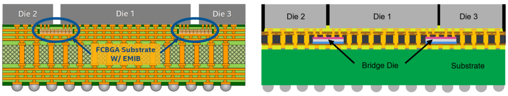
The industry has been working on methods that utilize bridging technologies for several years. Intel’s embedded multi-die interconnect bridge (EMIB) utilizes a bridge placed within the organic substrate to allow high-density routing without the use of silicon interposers. Amkor’s approach to this space embeds a bridge (silicon or other) into an HDFO design and this brings ultra-high-density design rules to the HDFO toolbox. Amkor refers to this technology as S-Connect. Figure 3 shows a comparison of these two design techniques.
When working with customers and industry partners the decision between silicon interposer, organic RDL HDFO, and bridge solutions like S-Connect, requires a trade-off analysis. The decision to go with bridges must address sourcing of the bridge die (with or without TSVs) and the silicon-integrated passive device (if warranted). The overall production readiness and maturity of each solution are also considered by the end customers. Silicon interposers are the most mature, as they have been in high volume manufacturing (HVM) for many years, followed by organic RDL with many successful qualifications complete and S-Connect, respectively. As systems become more complex, the need for integration may force solutions toward a bridge solution such as S-Connect.
There are three primary drivers for bridge technology. Bridge technology allows a reduced number of RDLs through the inclusion of silicon-based, high-density routing bridges for chiplet-to-chiplet or die-to-die routing, which in turn can lead to the potential for reduced system cost. Bridge technology also makes use of fab lithography that permits routing densities below 1 µm, which can facilitate finer bump pitch on the silicon top die. Finally, the use of the bridge technology allows for the creative use of embedded silicon integrated passive devices (IPD) in the same 3D location (see Figure 4), placed directly under the top die for optimal power delivery.
HDFO design and fabrication are available in die-first or die-last configurations. For simpler and smaller designs, die-first may be appropriate and a somewhat lower-cost approach. Amkor’s primary path for S-Connect designs uses a die-last approach to leverage expertise in die-last HDFO technology and to minimize the yield impact on customer silicon.
![[err-ad-fallback-title]](http://www.3dincites.com/wp-content/plugins/a3-lazy-load/assets/images/lazy_placeholder.gif)
Die-last S-Connect construction is composed of a base RDL with preformed tall copper pillars. The bridge die and other non-bridge dies (including IPDs) are placed face-up with smaller copper pillars. The wafer is molded and planarized to reveal all the copper pillars. Die placement capability is a crucial process requirement, which becomes more complex as the number of face-up bridge dies are placed in any given product. Additional RDL processing is then performed using an organic RLD process like HDFO with a die attach pad provided for die attachment. Chip-on-wafer assembly is then completed with a second mold and mold grind process. The wafer is then removed from the carrier and flipped over for back-side processing, where controlled collapse chip connection (C4) copper pillars are plated. At this point, the module formation is completed, and it fits into a common process used for other integrated modules.
Bridge die sourcing is another key aspect when contemplating S-Connect over other forms of heterogeneous integration. Customers may require the bridge to also have TSVs to provide power and ground into the I/O PHY. Sourcing and processing of these TSV-bearing bridge die will make the wafer-level fabrication of the S-Connect module more complex. Amkor has significant TSV process experience including a vast set of chemical-mechanical planarization (CMP)/backside passivation recipes to choose from that should minimize the development needed in the preparation of the TSV bearing bridge.
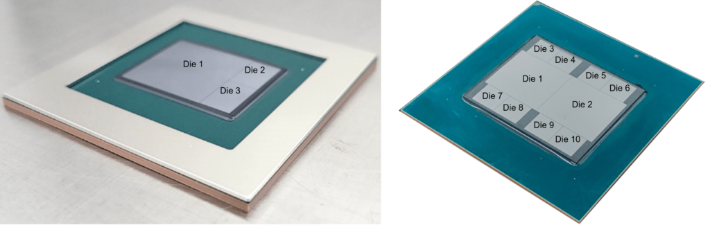
Presently, there are two internal TVs for S-Connect development. Development and internal qualification have been completed on three die modules comprising a larger die and two smaller (like high bandwidth memory (HBM)) die. The module has two bridge die and several test dies to mimic the placement of non-TSV bearing IPD die. On a larger scale, module TV development is occurring with 10 top die and 10 bridge die. This demonstration targets the very large modules, which benefit most from the use of silicon bridge die. Reliability results are expected on this TV in 2023. Figure 4 shows the two S-Connect test vehicles.
Amkor has been preparing for this next evolution of heterogeneous integration and we believe it will provide unique capabilities to augment the HDFO and silicon interposer solutions as more integration is required. With larger interposers (>2500 mm2), bridge solutions will help keep yields high as the highest density requirements (and highest potential yield loss) are on the bridge, which already has an extremely high yield.
Test Approaches
Amkor has been offering test services for heterogeneously integrated products since the beginning of these designs. The systemic approach of designing and evaluating the TV allows the test engineers to develop tests for critical aspects of the design before the live product.
There are a handful of test challenges that are common to all heterogeneous chiplet packages. Chiplet interconnect integrity is an important one. Signal and power delivery to every chiplet within the package requires careful layout, design, and test during the manufacturing process. The package material type impacts the interconnect performance between the chiplets and the pins exposed at the package level. This includes both static connection quality with continuity, leakage and transient ac timing, impedance matching, and signal crosstalk. In a carefully designed overall product architecture, design for test (DFT) access to all functional aspects of the product is an important consideration.
IEEE1838[“IEEE Standard for Test Access Architecture for Three-Dimensional Stacked Integrated Circuits,” in IEEE Std 1838-2019, vol., no., pp.1-73, 13 March 2020, doi: 10.1109/IEEESTD.2020.9036129.] is one such standard that helps during the architecture phase of the product. The thermal performance of each chiplet also impacts production testing. Thermal gradients due to non-uniform chiplet temperatures are common. A controlled, managed and repeatable production test environment ensures accurate feedback for future product design iterations and consistent yields.
Conclusions
Heterogeneous integrations using MCMs and the venerable 2.5D TSV silicon interposer approach have been in production for years. The transition to heterogeneous chiplet-based integrations is just beginning.
To integrate chiplets, a typical design must have a high-bandwidth interface between the die, and this normally necessitates fine bump pitches (≤55 µm), high signal rates, and short bus lengths. HDFO and S-Connect designs provide a cost-effective path for these integrations. Typical designs are less than 2500 mm2 but the trend is currently strong toward larger sizes and higher die counts.
For larger modules, the use of bridges makes sense. Large modules (>2500 mm2) using very fine-line RDL will cost more due to RDL yields. Using extremely high-yielding bridges to provide the finest routing between die, combined with lower density RDL elsewhere, will be a better economic tradeoff due to higher expected total yields. The bridge packaging solution is being developed and is targeted for customer qualifications in 2023 and 2024. HDFO chiplet integrations have been internally qualified and HDFO is ready for customer engagements and product qualifications. Best-in-class test services for heterogeneously integrated products complete the manufacturing process.
Please contact Mike Kelly at Amkor to discuss any of the options discussed above.
This article first appeared in the 2023 3D InCites Yearbook. Read the full issue here.