

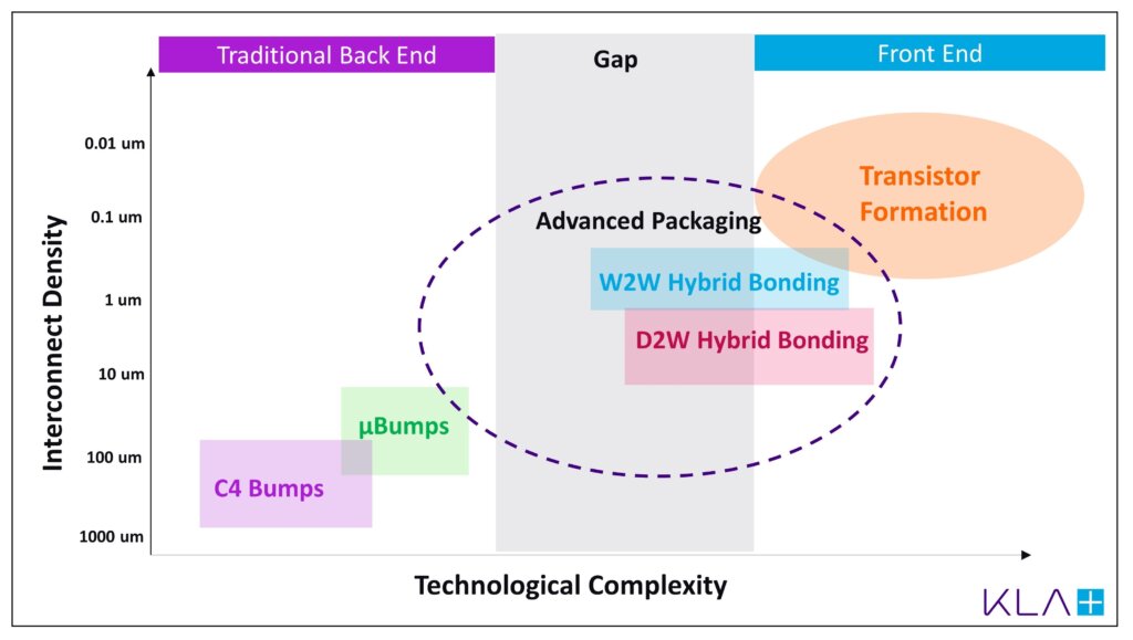
A Technology Chasm
Until recently, the world of IC fabrication was neatly divided into the distinct stages of front-end and back-end processing, with a large chasm separating them for both process complexity and economic value. The front end has been focused on increased processing or computing power and achieves this goal using highly complex process technologies to create ever-shrinking technology nodes. Once the devices are built, the wafer moves into the back-end phase, which is focused on connectivity, protection, and assembly. Here, wafers are prepped for assembly into their final packaging by establishing the necessary wiring and connection across devices. Historically, processing in this stage was not as advanced or economically valuable as the front end.
As a result, front-end advances in increasing transistor density and processing speed were pivotal in driving nearly all the improvements in computing — fueling Moore’s law. In recent years, however, thanks in part to the increased importance of memory in Big Data and AI applications, the semiconductor industry is at a point where processing speed is not the efficiency limiter. The efficiency of the entire finished package is critical and is limited by its least efficient component. Innovation is not new to the packaging industry, and with packaging processes now directly impacting overall device performance, the pace of invention has gained momentum. It is evident that huge gains can be achieved by increasing bandwidth or the rate at which data is pushed across devices. This shift has accelerated the adoption of some front-end patterning processes [lithography, etch, chemical mechanical planarization (CMP)] to introduce smaller feature sizes and more complex integration in packaging process flows to generate increased connectivity. As the value of advanced packaging in IC fabrication grows, the technology chasm between front-end and back-end shrinks.
Closing the Gap
As advanced packaging adopts complex processes from the front end, the clear separation that once existed between front-end and back-end wafer processing is starting to blur. This fuzziness is best embodied by packaging technologies like hybrid bonding, which due to its extremely demanding process complexity and small features, uses advanced, almost front-end-like processing (e.g., CMP) to result in improved electrical performance and increased interconnect density.
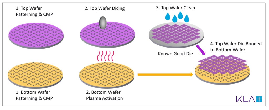
Hybrid bonding vertically connects die-to-wafers (D2W) or wafers-to-wafers (W2W) (Figure 2) via closely spaced copper pads. While W2W hybrid bonding has been in production for several years in image sensing, there is a strong industry push to expedite the development of D2W hybrid bonding. This development will further enable heterogeneous integration, which provides a powerful and flexible means to directly connect die of different functions, sizes, and design rules.
The dense copper interconnects associated with hybrid bonding leads to improved electrical performance and bandwidth, while direct die-to-die pad connectivity allows for a lower standoff height and thinner package size. Further, by using pre-inspected, diced known good die (KGD) during the bonding process for applications like 3D stacks in both high bandwidth memory (HBM) and logic, increased yield for the high-value package can be realized. This unrelenting march toward increased efficiency continues to fuel an offshoot of Moore’s law; closing the gap between what is considered front end and back end. Additionally, foundries and IDMs already skilled in front-end technology may be quicker to adapt to the high process complexity demanded by hybrid bonding; but OSATs will be working hard to catch up.
Hybrid Bonding Challenges
The use of front-end-like technologies in hybrid bonding is expected to provide huge performance and cost benefits, but not without unique challenges and opportunities for the industry. To keep yields economically favorable, the increased complexity brings about a greater need for metrology, inspection, and testing.
- Shrinking design rules and small copper pad dimensions require precise overlay to ensure pad contact and electrical connectivity
- Surface smoothness and precise dishing are required because roughness and imprecise dishing can compromise electrical connectivity
- Clean dicing and handling are required to prevent particulation, which can lead to the formation of costly yield killing voids after the bonding step
The successful implementation of D2W hybrid bonding in high volume will require resolution for each of these challenges. To meet alignment requirements, the pad-to-pad overlay must be measured through the top die accurately and precisely. The wafer surface profile after damascene pad formation must be measured with sub-nanometer precision to ensure that copper pads meet demanding recess or protrusion requirements. High sensitivity inspection to find all defects early in the process is required to verify that the die surface remains clean for a successful void-free bonding process step.
KLA’s Solution for Hybrid Bonding Process Development
The recently launched Kronos™ 1190 wafer-level packaging inspection system is targeted at enabling process development for hybrid bonding, with its high sensitivity darkfield channel for small particle detection and brightfield capability that can detect residue defects. The system can inspect a wide variety of substrate types such as a whole wafer, diced wafer on film frame, and reconstituted wafer-on-carrier to support a broad range of process flows.
In addition to defect inspection, it may be beneficial to use non-mechanical dicing methods like plasma dicing because of much lower particle contamination levels. KLA’s wide range of advanced process control and process-enabling solutions and decades of leadership in front-end process control uniquely position our equipment to address hybrid bonding challenges at a superior cost of ownership.
About the Authors
 Swati Ramanathan, Ph.D. is a product marketing manager in KLA Corporation’s LS-SWIFT Division, Global Products Group, where she shapes products to meet the diverse inspection needs of the advanced wafer-level packaging market. Ramanathan’s nine-year industry experience spans both marketing and technical aspects of semiconductor wafer inspection. Her areas of specialty include spectroscopy, semiconductor nanostructures, and condensed matter physics.


Steve Hiebert is senior director of marketing for the LS-SWIFT Division of KLA Corporation’s Global Products Group. He is responsible for driving business initiatives in the advanced packaging and optical devices market segments. With over 20 years at KLA, Steve’s experience spans product and strategic marketing for wafer inspection and metrology as well as corporate marketing roles.
This article first appeared in the 2021 Yearbook. Find the full issue here.


