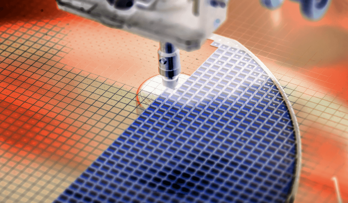
Modern-day applications such as cloud computing, high-performance computing, artificial intelligence (AI), data centers, and future 6G systems are driving the implementation of advanced packaging schemes such as system-in-package (SiP), 3D-stacking, 2.5D-Interposers, and more. These schemes are not only replacing Moore’s law in driving semiconductor performance but at the same time are reducing the footprint of the assembled devices. With these implementations comes a continuous need to scale interconnect dimensions and pitches.
Typical interconnects are composed of solder-capped copper pillars, which exist either on a chip, on a substrate, or in some cases on both sides. The finest pitches in more recent advanced packaging applications range from 25 – 80 µm and are implemented either through a conventional mass reflow (MR) or via a more sophisticated thermal compression bonding (TCB) process. The pitch and dimension scaling below 50 µm, though very enticing, comes with challenges that cannot always be surmounted using traditional flux-based processes.
Flux-less TCB using in-situ Formic Acid Vapor Delivery
One of the consequences of pitch and dimension scaling is the reduction of stand-off height between the chip and the substrate. This makes the post-bonding flux residue removal that is needed to achieve very high yields very challenging.
Furthermore, the flux burn-off from the substrate surface limits the highest achievable substrate temperature and duration of exposure especially if the materials e.g., a 300 mm wafer, need to spend a long time i.e., 0.5 hours to 4 hours on a hot chuck. This is problematic with applications such as memory, where the highest temperature on the chip side is limited to 275 °C to 300 °C, as a higher chuck temperature is needed to achieve sufficient bond-line temperatures. Under these boundary conditions, conventional flux-based TCB processes cannot achieve the expected bond quality or throughput.
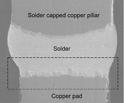
In recent years, a proprietary flux-less TCB technology was productized that can address these issues by avoiding flux altogether. This flux-less technology is based on generating a localized reducing environment at the target bonding region by using formic acid vapor. In-situ application of the reducing gas ensures the removal of existing oxides from both the chip and substrate just prior to the TCB process. In addition to that, this entire process is carried out in an inert chamber filled with nitrogen gas, which minimizes the rate of oxidation during prolonged heat exposure. Essentially, the flux-less TCB process can achieve higher yields and further enable higher substrate temperatures, which can potentially reduce the required thermal budgets on the chip side. Flux-less bonding has been successfully demonstrated for both solder-to-copper and solder-based interconnects. An example of solder-to-copper contact is shown in Figure 1. The interface shows excellent intermetallic growth.
Cu-Cu Thermal Compression Bonding
This proprietary flux-less TCB technology is primarily targeting solder-based fine pitch applications i.e., 12 – 80 µm, but there is a natural path for its applicability towards Cu-Cu TCB as well. The inclusion of the already available inert bonding environment along with in-situ reducing gas delivery are two major technologies that enable successful bonding of mating copper surfaces. We believe that the Cu-Cu TCB interconnect solution has major benefits between about 5 – 20 µm pitch.
In the past few years, serious efforts have been made to transition from solder-based contacts to pure Cu-based contacts using hybrid bonding, however, the costs associated with infrastructure, equipment, and material preparation make it a very expensive solution. Researchers have published extensively on this Cu-Cu thermal compression bonding technology for the past several years as the technology matured. They have also identified critical factors affecting the Cu-Cu bonding, including material preparation issues e.g., copper pillar topology (height and diameter), surface oxide removal, surface roughness, surface planarization, and the TCB parameters such as temperature, pressure, bonding times, etc. Understanding both material preparation and TCB factors has allowed us to develop and demonstrate successful Cu-Cu bonding processes.
Factors Affecting Cu-Cu TCB
The mechanism of Cu-Cu bonding is a solid-state diffusion process that requires the removal of surface oxides prior to interfacial contact using e.g., an in-situ reducing gas such as formic acid vapor. The oxide-free Cu surfaces come in intimate contact and allow the solid-state diffusion of copper atoms across the bonding interface.
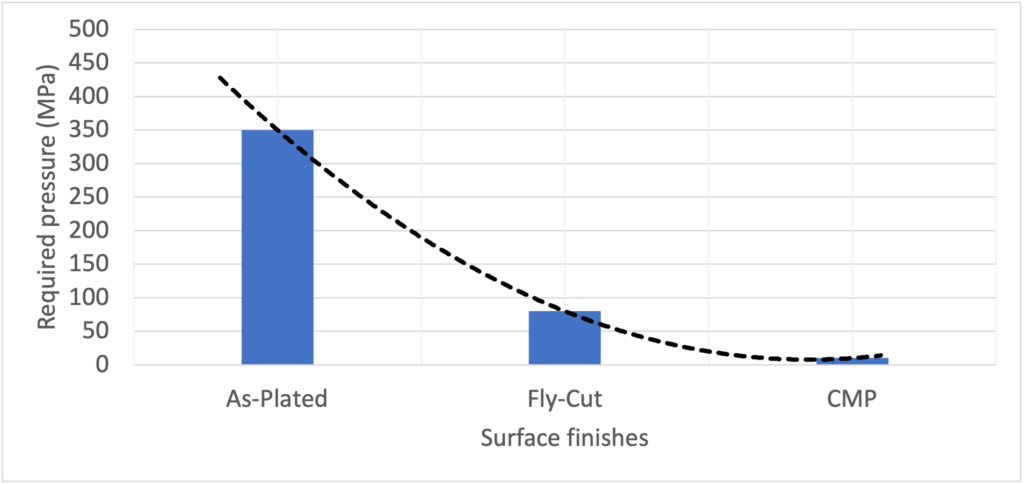
A combination of temperature and pressure during TCB causes the copper to plastically deform thus removing interfacial asperities. Furthermore, the CMP process can be deployed to achieve higher surface flatness i.e., ≤ 10 nm to begin with. Roughness control is crucial since it determines the pressure required to remove asperities. In general, the higher the surface roughness is at the interface, the higher the pressure required to flatten the asperities.
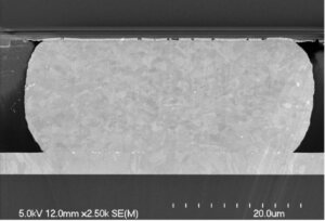
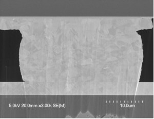
Figures 2 to 4 show Cu-Cu bonds formed using electroplated (100-200 nm), fly-cut (15-20 nm and CMP-planarized (1-2 nm) copper pillars, respectively, using this flux-less technology. Note that CMP planarized test vehicles were bonded by UCLA CHIPS using a K&S TCB tool equipped with formic acid delivery capability [1].
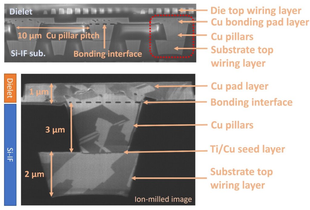
Over the years, K&S has showcased Cu-Cu implementation for various surface finishes along with critical TCB parameters such as pressure. Figure 5 shows an extremely potent relationship between applied pressure and localized surface roughness. Co-planarity of both chip and substrate is another factor since part of the applied pressure is utilized to bring two entities in intimate contact.

A high-yield Cu-Cu TCB process can be successfully performed in a Class-1000 clean room, which is nearly impossible for a competitive hybrid bonding type process. Cu-Cu TCB is less sensitive to foreign material interference although it is important to keep the bonding environment as clean as possible since minimizing foreign interference will always guarantee higher yields. Material properties of the copper can further influence the solid-state bonding process i.e., pressure and temperature requirements can vary. For example, heat treatment of copper beyond its recrystallization temperature reduces the internal stress and makes the copper more ductile, thus changing the required bonding pressure.
It is worth mentioning that certain crystallographic orientations such as (111)-Cu have very high diffusivity i.e., orders of magnitude higher than e.g., (100)-Cu which can affect the solid-state diffusion process during grain growth. Despite the benefits that this special crystal orientation brings along, randomly oriented copper works successfully during Cu-Cu TCB.
Underfill Requirements and Reliability
A reliable Cu-Cu bond is generally achieved when mating surfaces are well-contacted during the TCB process and can be realized with a pillar/pad construction that is planar with the surrounding dielectric or by making copper pillars slightly proud e.g., 0.1-1.5 µm from the chip or substrate surfaces. The protruding pillar bonding process can be more straightforward, however, leaves a small chip-to-substrate gap e.g., 0.1-2 µm. None of the established underfill materials or methods has so far resulted in filling the tiny gap. Therefore, K&S and UCLA CHIPS are collaborating to develop a CVD-based underfill method.
For demonstration purposes, a 10 nm layer of aluminum oxide (Al2O3) was deposited using the atomic layer deposition (ALD) method, which conformally coated a 1.5 µm chip-substrate gap on a 4 mm2 test device with a 10 µm interconnect pitch [1]. UCLA also performed highly accelerated stress tests (HAST) at 130 °C and 85 % relative humidity for 96 hours according to JDEC JESD22-A118 test standard and showed that ALD-encapsulated assemblies exhibited high reliability as electrical resistance change was less than 10%.
Unfortunately, there is no reliability data yet available for these tiny-gaped assemblies or general for Cu-Cu thermal compression bonding; therefore, reliability data will be published in the future. K&S has also investigated if Cu-Cu TCB bonding can be applied to hybrid-like structures i.e., where both metal and oxide are coplanar. Through initial experiments, we have concluded that we can also achieve higher yields for such surface topologies. During the TCB process, the copper surface on the chip side expands due to elevated temperature i.e., 300 – 400 °C, and makes intimate contact with the opposing substrate surface, which is typically at a much lower temperature range e.g., 100 – 200 °C. Under sufficient pressure and temperature, these protrusions are enough for solid-state diffusion of copper atoms and grain growth across the interface during TCB. Additionally, the coplanar copper and oxide structures would not require any underfill to achieve high joint reliability.
Conclusions
We conclude that formic acid vapor-based flux-less TCB is a viable option for solder-based fine-pitch applications i.e., 80 – 12 µm, and can be further extended to a solderless Cu-Cu TCB process down to 5 µm pitch. It provides a unique advantage of achieving higher yields compared to solder-based processes and further enables much higher chuck temperatures for unique applications e.g., memory where allowed chip-side temperatures are only limited to 275°C to 300 °C. Solder-based flux-less TCB has already been adopted as a high-volume manufacturing process and we expect its widespread application to more advanced solderless Cu-Cu TCB processes as well.
Reference
1. K. Sahoo, H. Ren and S. S. Iyer, “A High Throughput Two-Stage Die-to-Wafer Thermal Compression Bonding Scheme for Heterogeneous Integration,” 2023 IEEE 73rd Electronic Components and Technology Conference (ECTC), Orlando, FL, USA, 2023, pp. 362-366, doi: 10.1109/ECTC51909.2023.00067.