Live from “Silicon Desert”: The news is all about huge spending by TSMC and Intel. Investment in advanced packaging (2.3/2.5/3D including chiplets) is increasing. As a 5nm design effort tops $500M and photo tools approach $150M, it was necessary to bust up systems-on-chip (SoCs) into re-partitioned systems – where functions that don’t need sub 10nm processes are off-boarded to older process nodes, along with specialty technologies beyond core logic (such as PMIC, RF, analog/mixed-signal). A recent high-water mark case making headlines is Intel’s Ponte Vecchio (47 active chiplets).
Advanced packaging sources include vertically integrated IDMs, foundries, and OSATs. Chiplet approaches are ideal for some requirements, but they are not for the faint of heart and pose many test challenges. This summary, based on large processor-based systems, will break this down into:
- Realistic analysis/decision-making
- Leveraging Standards when forming test plans
- New work/way (s) forward in test approaches
Realistic Analysis / Decision Making
Many design tradeoffs and test challenges are part of overall decisions around architecture and to what degree chiplets should be used. Test teams must work closely with design and business teams to make decisions to get quality products to market with the right return on investment (ROI). Many test tradeoffs and complexities will help avoid catastrophic surprises such as excessive test times, too many insertions, staffing, lack of coverage, test-related risks that are under-scoped and become issues, and/or schedules that impact time to market.
Chiplet Advantages
- Integration of heterogeneous die
- Higher yield (reduced die size of core- and higher-yielding chiplets based on older nodes)
- Help meet power-performance requirements
- Process large amounts of parallel data with high bandwidth memory (HBM)
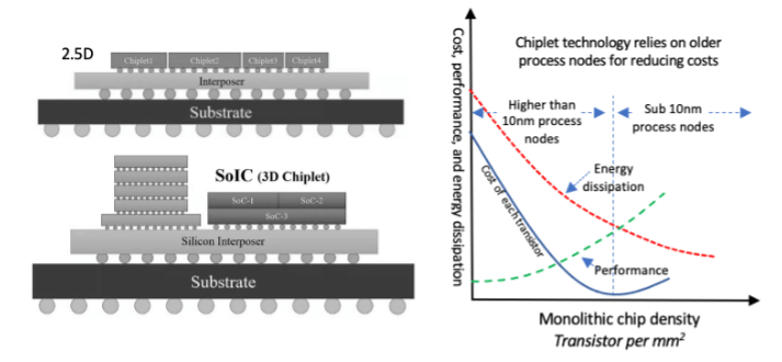
Recently, R. Zamon summarized a 10nm tipping point.1 As opposed to intricate chiplet-based systems, a simple system on a board (SoB) with multiple monolithic ICs and SMDs &/or “simple” SiPs can be more effective (Figure 1). Zamon further contends that chiplets produced using older nodes suffer from multiple limitations including performance, latency, heat dissipation, and package size. Chiplets may be new designs, old designs (presumably at older process nodes), 3rd party IP, or derived from other sources (such as a chiplet market). All this makes multi-variate decisions difficult to make.
Advanced packaging leads to many electrical and reliability issues and risks that will need to be screened out by test and reliability stresses.
Product Risks and Issues Lead to Chiplet Test Challenges1,2,3
- Contact resistance and capacitive loading from pillars and bumps
- Crosstalk and increase noise in substrates and interposers
- Insertion and return losses – especially through-silicon and through-mold vias (TSV, TMV)
- Electro-magnetic effects
- High speed die-to-die interfaces (D2D) are hard to achieve
- Thermal issues with interconnect and underfill layers, bulk silicon, and heat sink
- Mechanical stress of substrates, interposers, die, and package
- Latent defects
- System permutations/options – cores, memory, peripherals in many configurations
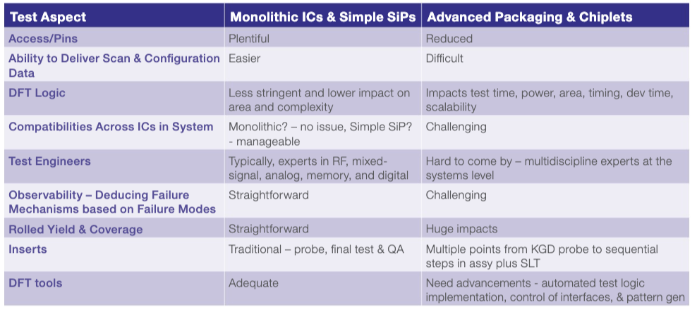
Table 1 shows test challenges and a comparison of product types.3
Leveraging Standards
Test engineers need to become more fluent with top-down and bottom-up standards. Top-down standards include:
- ODSA – open D2D interface guideline
- UCIe™ – Universal Chip Interconnect Express – see my blog [4] for details
- 3DFabric Alliance – TSMC effort
Bottom-up standards refer to structural and functional methods – some have been around a long time (BIST, scan) but have become more important – others are emerging, such as IEEE 1838.
- IEEE Specifications
- x – access ports & boundary scan architecture
- 1500 – embedded core test(s)
- 1687 – access to and operation of embedded instrumentation
- 1838 – die centric standard intended for multi-die packages
Test configurations are then delivered via serial and broadcast networks (1687 & 1500) with 1838 delivery of configuration data through test-access-ports to reach embedded die

New Strategies
Beyond architecture and standards, more invention is needed. There will be a learning curve. Let’s look at a few new approaches:
- Hierarchical methodology: divide and conquer by dividing the design into smaller hierarchical partitions for quick DFT sign-off (insertion, mode setup, pattern gen, and verification.3
- Use package broadcast, on-die scan comparators (ODSC), and “accelerated fly-overs” to leverage reuse, shorten development times and reduce bring-up overhead.5
- Redistribute content such that a system-level test (SLT) is performed right after final packaging – then failing units move onto a final test &/or stresses to enable faster learning cycles – good units go on to the final test. 2
- Accessing and testing die through primary dies with higher pin accessibility using an efficient data delivery mechanism.3
- Use a known-good processor and interconnect types from the actual design (silicon bridge, interposer, other) on the load board to test the socketed chiplet DUT.
- On board/in-system telemetry, such as proteanTec
- Greater use of the adaptive test, assembly/test monitoring, end-to-end traceability; unit-level traceability for ‘big data’; design/fab/packaging/final and system level test real-time adjustments; and comprehensive analytics, such as from PDF Solutions.
Summary
For high-end processors with onboard memory, chiplets offer a way to reduce cost, improve some performance(s) and leverage IP from multiple companies. At the same time – simple wire bond packages continue to make up 70% of the industry’s volume and chiplet designs are not always appropriate versus monolithic ICs, simple SiP, and SoB. Realistic analysis and decision-making are needed at the design start – with test considerations in mind. Without this, there can be huge consequences to cost, quality, and time to market. Existing and new standards should be followed closely and as with any new technology introduction, learning cycles, and ingenuity are the way. It will be interesting to see how widely chiplet technology is adopted and to what extent it goes beyond the major IDM realm.
This article first appeared in the 2023 3D InCites Yearbook. Read the issue here.
References
- R. Zaman – The Waves – “Chiplet Technology — a Weak Reinvention Core?” – Dec 5, 2022
- V. Pancholi – MEPTEC Road to Chiplets – “Test Impacts of Multi-Die Packages” – May 10-12, 2022
- R. Singhal – SemiEngineering – “A Practical Approach to DFT for Large SoCs and AI Architectures, Parts I and II” – Jan 11 & Mar 18, 2022
- M. Berry – 3D InCites – “Update on the UCIe™ from ITC 2022” – Oct 6, 2022
- A. Margulis et.al – ITC 2022 – “Chiplet Level Test Parallelism for 3D Stacking Projects”
Other interesting reads:
A.Mutschler – “Designing for Multiple Die” – SemiEngineering – Dec 21, 2022
From ITC 2022
- Shalf – “The Future of High-Performance Computing Beyond Moore’s Law”
- Ranganathan – “Make Computing Count: Some Grand Opportunities for Testing”
- D.D. Sharma – “Road to Chiplets: UCIe™”