Latest Posts - Page 4
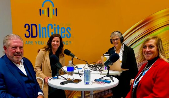
Live from SEMICON West Hybrid 2021 – It’s the 3D InCites Podcast!
I can’t tell you how much fun I had last week at SEMICON West! My favorite part has always been...SEMICON West… It’s Back! Community Member Preview
We presume all are excited about the upcoming SEMICON West show. I know we sure are! Be sure to stop...
From Cubes to Chips: One Engineering Student’s Journey
It all started with a Rubik’s Cube… When I was in middle school, I liked to struggle with new concepts...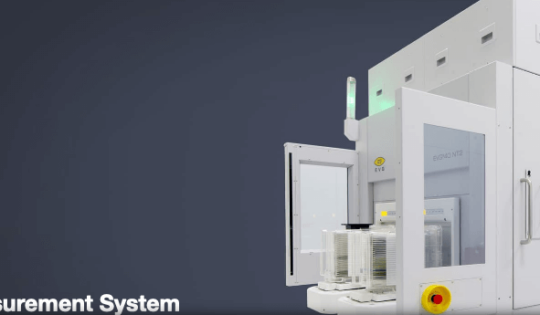
EV Group Brings High-speed High-precision Metrology to 3D Heterogeneous Integration
EVG®40 NT2 offers breakthrough metrology performance to accelerate implementation of wafer- and die-level hybrid bonding and maskless lithography FLORIAN, Austria,...
SEMICON Europa Member Preview
SEMICON Europa is back! On the agenda? The latest innovations and smart applications powering the next wave of semiconductor industry...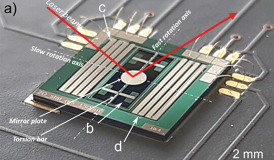
Cooperation of ZKW Group with Silicon Austrian Labs, Evatec, EV Group and TDK Electronics advances light projection technology
WIESELBURG, Austria, August 25, 2021—Together with research partners Silicon Austrian Labs, Evatec, EV Group and TDK Electronics, ZKW is working...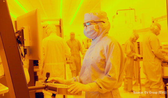
EV Group Launches First-of-its-Kind Step-and-Repeat Mastering Services for Nanoimprint Lithography
EVG S&R Mastering Shop™ further lowers barriers to adoption of nanoimprint lithography for wafer-level and panel-level production applications such as...
Introducing the 3D InCites Podcast
Over the past month, you may have noticed a new addition to the 3D InCites platform. The 3D InCites Podcast...
ECTC 2021 Features the Hottest Topics and Trends in Microelectronics
For the second time in its 71-year history, ECTC will be presented as a virtual conference, opening Tuesday, June 1,...

Die-to-Wafer Bonding Steps into the Spotlight on a Heterogeneous Integration Stage
The semiconductor industry is currently undergoing the most radical change in its history. Many new applications such as artificial intelligence...
YES Joins Forces with EV Group
YES EcoCoat™ to be installed at EVG’s NILPhotonics® Competence Center in Austria FREMONT, Calif. – Apr 19, 2021YES (Yield Engineering...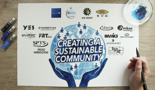
2021 3D InCites DEI Fundraiser a Success; Thank You Sponsors
We took our annual mural project online this year! Illustrator Ronna Encarnacion created this original watercolor to reflect the importance...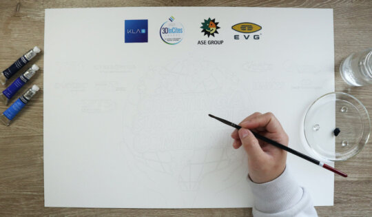
3D InCites Mural Project To Seed New DEI Fund
For the last several years, we held the 3D InCites Mural Project, in conjunction with the 3D InCites Awards, in...
3D InCites Community Members SEMICON China 2021 Preview
SEMICON China attracts the world’s leading technology companies who design, develop, manufacture, and supply the technologies to manufacture the microelectronics...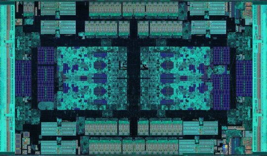
IFTLE 478: Chiplet Nomenclature; EV Group/ASM Support D2W Hybrid Bonding
On Definitions and Buzzwords Long-time readers of IFTLE know that I’m sensitive about nomenclature and buzzwords. For instance: “nanotechnology” and...
Join 3D InCites and Our Members at SEMI’s Technology Unites Global Summit
While most of SEMI’s global events went virtual in 2020, SEMICON Europa was straight-up canceled. While I was disappointed, since...ASM Pacific Technology and EV Group Join Forces to Enable Industry’s First Ultra Precision Die-to-Wafer Hybrid Bonding Solutions for 3D-IC Heterogeneous Integration
Joint Development Program will offer highly configurable, ultra-precision end-to-end hybrid bonding solutions to suit various applications, with optimal line balancing...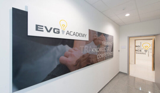
EV Group Establishes State-of-the-Art Customer Training Facility at Corporate Headquarters
EVG Academy doubles the amount of training space and technical trainers; provides training on every class of EVG equipment and...