
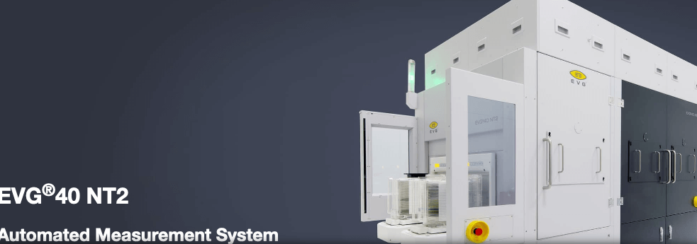
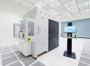
EVG®40 NT2 offers breakthrough metrology performance to accelerate implementation of wafer- and die-level hybrid bonding and maskless lithography
FLORIAN, Austria, November 15, 2021—EV Group (EVG), a leading supplier of wafer bonding and lithography equipment for the MEMS, nanotechnology and semiconductor markets, today unveiled the EVG®40 NT2 automated metrology system, which provides overlay and critical dimension (CD) measurements for wafer-to-wafer (W2W), die-to-wafer (D2W) and die-to-die (D2D) bonding as well as maskless lithography applications. Designed for high-volume production with feedback loops for real-time process correction and optimization, the EVG40 NT2 helps device manufacturers, foundries and packaging houses accelerate the introduction of new 3D/heterogeneous integration products as well as improve yields and avoid scrapping of highly valuable wafers.
EVG will showcase the EVG40 NT2 system for the first time at the SEMICON Europa tradeshow, taking place November 16-19 at the Messe München in Munich, Germany. Attendees interested in learning more can visit EVG in Hall B1, booth B1460.
Heterogeneous Integration Roadmap Driving New Metrology Needs
As traditional 2D silicon scaling reaches its cost limits, the semiconductor industry is turning to heterogeneous integration—the manufacturing, assembly and packaging of multiple different components or dies with different feature sizes and materials onto a single device or package—in order to increase performance on new device generations. In W2W, D2W and D2D bonding, tight alignment and overlay accuracy is required to achieve good electrical contact between the interconnected devices. As interconnect pitches become tighter with each new product generation, wafer and die bond alignment and overlay processes must also scale accordingly, with greater accuracy and more frequent measurements to identify process problems when they occur in order to provide corrective action or the possibility for rework, leading to higher production yields. Maskless exposure, an innovative lithographic approach for 3D/heterogeneous integration, requires increasingly precise pattern fidelity and pattern overlay on highly warped and distorted wafers that often incorporate shifted dies—driving the need for metrology that delivers crucial information on die position.
“Process control is increasingly critical for leading-edge 3D and heterogeneous integration applications,” stated Dr. Thomas Glinsner, corporate technology director at EV Group. “The EVG40 NT2 represents a major breakthrough in metrology performance to meet the new demands for the advanced packaging industry. It provides not only greater overlay accuracy but also a significant boost in throughput to enable higher measurement density per wafer, giving more detailed feedback on hybrid bonding performance, for example. This new metrology solution rounds out EVG’s comprehensive portfolio of process solutions for 3D/heterogeneous integration, and complements our existing EVG40 NT system, which remains the de facto bond metrology standard for MEMS and complex photonic devices. The EVG40 NT2 is already playing a key role in several joint development projects underway at EVG’s Heterogeneous Integration Competence Center™.”
High-Precision, High-Throughput Metrology Performance
The EVG40 NT2 system provides highly precise measurements of critical bonding and lithography process parameters for current and future leading-edge 3D/heterogeneous integration applications. These measurements include: alignment verification and monitoring for W2W, D2W, D2D and maskless exposure processes; CD measurement; and multi-layer thickness measurement. It is a highly scalable system that features multiple measurement heads and a high-precision stage designed for high-throughput and high-accuracy (down to the low single-digit nm range) bonding and maskless exposure alignment verification. For alignment verification, the EVG40 NT2 generates an overlay model that can be used in a feedback loop for improving overall alignment. This reduces systematic errors and results in increased production yields. The system is compatible with multiple line optimization concepts for overlay feedback and die position feed-forward required by next-generation fabs supporting Industry 4.0 manufacturing.
![[err-ad-fallback-title]](http://www.3dincites.com/wp-content/plugins/a3-lazy-load/assets/images/lazy_placeholder.gif)
Product Availability
EVG is now accepting orders for the new EVG40 NT2 automated metrology system, and offering product demonstrations at EVG’s Heterogeneous Integration Competence Center at its headquarters in Austria. For more information, please visit https://www.evgroup.com/products/metrology/.
About EV Group (EVG)
EV Group (EVG) is a leading supplier of equipment and process solutions for the manufacture of semiconductors, microelectromechanical systems (MEMS), compound semiconductors, power devices and nanotechnology devices. Key products include wafer bonding, thin-wafer processing, lithography/nanoimprint lithography (NIL) and metrology equipment, as well as photoresist coaters, cleaners and inspection systems. Founded in 1980, EV Group services and supports an elaborate network of global customers and partners all over the world. More information about EVG is available at www.EVGroup.com.

