
On Definitions and Buzzwords
Long-time readers of IFTLE know that I’m sensitive about nomenclature and buzzwords. For instance: “nanotechnology” and “internet of things” are buzz words that are being used way too loosely and have little meaning. I’m OK with 2.5D because I was there when it was first uttered (as a joke) and we all know what it means. However, don’t use 2.1D or 2.3D around me unless you’re intentionally trying to start a heated argument.
Thus, you can understand how the broadening of the new buzzword “chiplet” is also beginning to rub me the wrong way.
With that said IEEE Electronics Packaging Society (EPS) was asked to officially comment on the definition of chiplets. I was asked to be part of the committee deriving the definition, which was officially released by VP of technology Dave McCann in the EPS Feb newsletter. I’m including it here to broaden its exposure.
“The naming of new technologies can be difficult and often inaccurate. Over time, standards are developed and language becomes aligned. The cost of leading-edge nodes, combined with the lack of scaling of significant design blocks (ex: analog) and die sizes reaching reticle size, is driving disaggregation (splitting up) of chip functions into their best price/performance nodes requiring new technologies to interconnect these functions. We are voicing our support in naming these small IP blocks “chiplets”. It is not a perfect name but fits into our vernacular well and is gaining acceptance in our industry. Our definition of “chiplet”, and what it is not, follows. We appreciate your inputs.”
~ David McCann EPS, VP of Technology
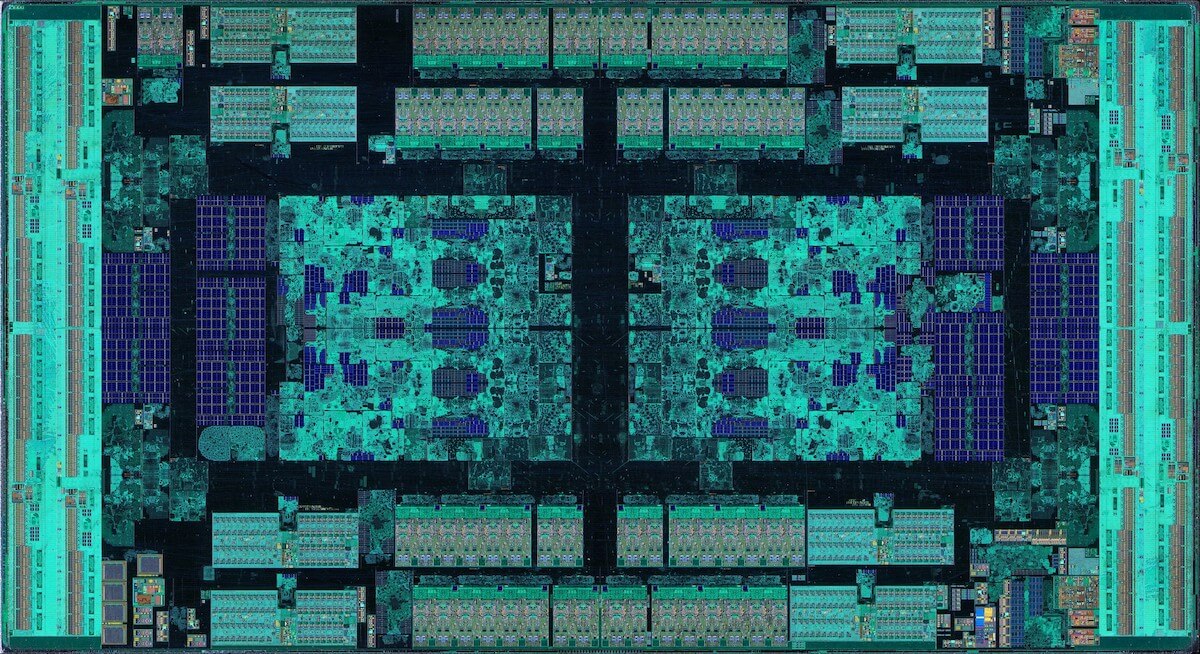
Chiplet is not a package type, it is part of a packaging architecture. It is an integrated circuit block that has been specifically designed to communicate with other, similar chiplets, to form larger more complex ICs. Thus, in large and complex chip designs the design is subdivided into functional circuit blocks, often reusable IP blocks, called “chiplets”, that are manufactured and recombined on high density interconnect.
Historically, the need for multiple chips to deliver a specific function was driven by the reticle limit which dictated the maximum size of a chip possible to be fabricated. Designs that exceeded the reticle limit were split up into smaller dies to be manufacturable. As technology continued to enable increased integration, multiple dies were merged into single, more complex ICs. Thus, the origin of the term “system” on a chip or SoC.
More recently, economics has caused a reversal of that trend. As the industry moves to smaller process nodes, costs for yielding large dies increases. The desire to move to a chiplet-based design has been driven by the increasing cost of manufacturing devices on leading-edge process nodes. Compared to a 250 mm² die fabricated on a 45nm process, a 16nm process more than doubles the cost/mm², and a 7nm process further doubles that to 4x the cost per yielded mm². Moving to the 5 nm and even 3 nm nodes, is expected to make this even worse.
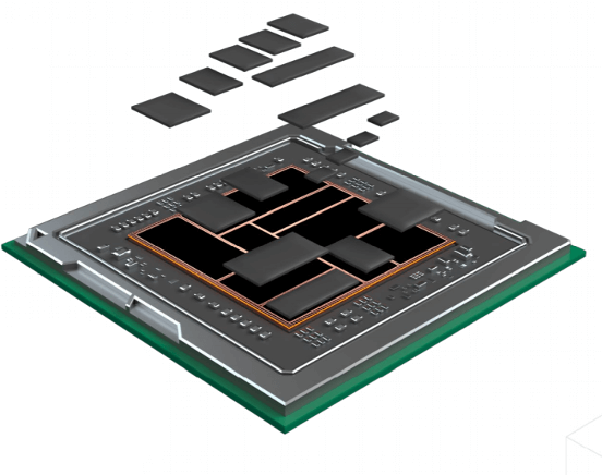
The chiplet solution can be used to ease the economics of manufacturing such chips, with large numbers of transistors, at state-of-the-art nodes. In chiplet-based design, the chip is broken down, by function, into multiple smaller chiplets and only the chiplets that require the latest node are made in that node (Figure 1). Some envision, that in time, the greater use of chiplets will drive the package to become the new SoC, and chiplets become the new “IP”. However, for this to be viable across packaging companies, there must be standard/common communication interfaces between chiplets. There are several solutions today, but standards must be chosen.
Finally, chiplet nomenclature SHOULD NOT be used to describe: a) tiny chips, b) a packaged die, c) a package type, d) or chips combined in a multichip module (MCM) or system in package (SiP) unless they meet the criteria given above.
D2W Bonding Update
Readers of IFTLE will know that we have been tracking the technology known as hybrid bonding technology since its earliest conception by Ziptronix some 20+ years ago. See IFTLE 475 for our latest discussions. It is a perfect example of how really new technologies take time, sometimes decades, to become accepted by the wider community.
Many believe that die-to-wafer (D2W) hybrid bonding is pivotal to transform redesign of SoC devices into 3D stacked chips via combining chips with different process nodes (aka: heterogeneous integration – or HI) into advanced packaging systems to power new applications such as 5G, high-performance computing and artificial intelligent (AI).
As we have discussed previously, hybrid bonding has become a process step found on nearly all advanced packaging roadmaps. One of the equipment companies that has been along for the ride when it comes to hybrid bonding technology has certainly been EV Group.
Together, ASM and EV Group Enable D2W Hybrid Bonding Solutions
ASM and EV Group (EVG) recently announced the signing of a JDA to co-develop die-to-wafer (D2W) hybrid bonding solutions for 3D-IC.
D2W bonding capabilities require well-matched equipment partners from the wafer fab and assembly space to come together to deliver solutions for the next level of package scaling. This is what this JDA aims to achieve. Both companies are leaders in their respective areas, with EVG’s die preparation technology and front-end cleanliness for die-to-wafer hybrid bonding, and ASMPT’s ultra-high precision bonding of extremely thin dies. Under the JDA, ASMPT will provide its precision die-bonding capabilities, while EVG will provide its die preparation (cleaning and activation) and wafer bonding capabilities in the form of the EVG®320 D2W system for direct-placement die-to-wafer bonding as well as the EVG GEMINI® FB configured for collective die-to-wafer integration flows.

The goal is for system designers to be able to mix and match chiplets and optimally connect them by using ASMPT’s ultra-high precision (0.2µm) die placement, along with EVG’s die-to-wafer hybrid bonding and fusion technologies, to achieve comparable or even better performance than SoC methodologies.
As part of the JDA, ASMPT and EVG will leverage their core competency centers in Europe and Asia to speed up the development of lead customer programs, with an eventual offering of highly-configurable modular systems to suit a full spectrum of integration and process requirements.
In 2017 imec and EVG achieve 1.8µm accuracy in pitch overlay for wafer-to-wafer (W2W) hybrid bonding
Later that year, EVG announced 300-mm W2W direct hybrid bonding with 1µm pitch. (Figure 1)
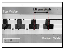
The copper/oxide hybrid bonding process, a key enabler for 3D high-density IC applications, was demonstrated in Leti’s cleanrooms using EVG’s GEMINI®FB XT fusion wafer bonding system. The system achieved overlay alignment accuracy to within 195nm (3-sigma) overall, with mean alignment results well centered below 15nm. Post-bake acoustic microscopy scans of the full 300-mm bonded wafer stack, as well as specific dies, confirmed a defect-free bonding interface for pitches ranging from 1µm to 4µm with optimum copper density. This work was reported in a paper “1 µm Pitch Direct Hybrid Bonding with <300nm Wafer-to-wafer Overlay Accuracy,” which was presented at the 2017 IEEE S3S Conference.
In 2020, EVG unveiled a hybrid D2W bonding activation solution for 3D HI.
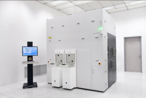
The system incorporates all critical pre-processing modules needed for D2W bonding, including cleaning, plasma activation, die alignment verification, and other essential metrology, and can be operated as a stand-alone system or integrated with third-party pick-and-place die bonding systems.
In collective D2W bonding, singulated dies are placed on collective die carriers and are then transported to a target wafer for die transfer where a W2W hybrid or fusion bonding system, such as the GEMINI FB, is used to bond the dies to the target wafer. In direct placement D2W (DP-D2W) bonding, the singulated dies are bonded to the target wafer one by one using a pick-and-place flip-chip bonder. Plasma activation and cleaning of the surfaces of the dies on the handler wafer are essential steps for establishing a high-yielding bond and electrical interface between the dies and target wafer. This is where the EVG320 D2W activation system comes in.
The EVG320 D2W system fills a critical need for innovative process solutions that can accelerate the deployment of heterogeneous integration and enable new generations of devices and systems such as high-bandwidth memory (HBM), logic-on-memory, chiplets, segmented and 3D system on chip (SoC) devices, and 3D stacked backside-illuminated CMOS image sensors.
For 20 years, EVG has continually set new standards for wafer-to-wafer hybrid and fusion bonding with the largest installed base of wafer bonding solutions worldwide,” stated Paul Lindner, executive technology director of EV Group.


