
IME – Hybrid Bonding Studies
Singapore’s Institute of Microelectronics – IME / AStar – was certainly the most prolific presenter at the conference. In their presentation, “Wafer Level Fine-Pitch Hybrid Bonding: Challenges and Remedies”, they review in great detail processing issues prevalent in hybrid bonding.
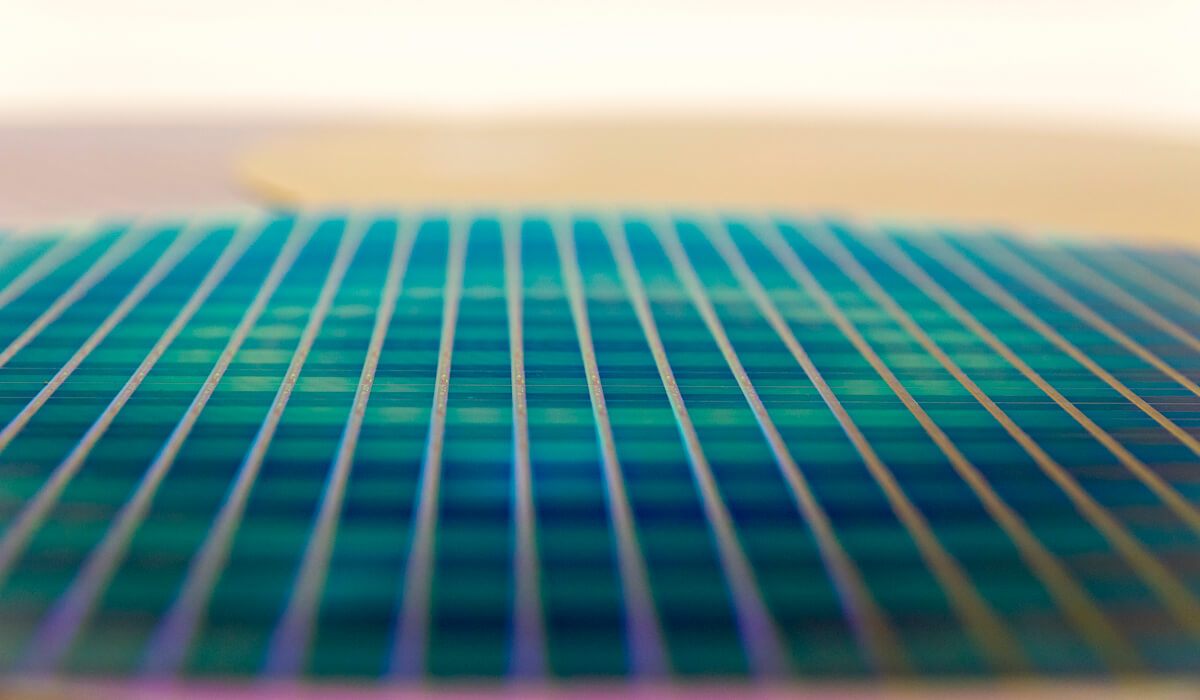
Wafer-level fine-pitch hybrid bonding, first discussed and patented by Paul Enquist and his colleagues at Ziptronix in the early 2000s, has emerged more than a decade later as a key technology in three-dimensional integrated circuits (3D- IC). Hybrid bonding involves simultaneous metal and dielectric bonding. It provides both mechanical support and dense electrical interconnects between bonded wafers. Cu is the commonly used interconnect. It has been the driving force for the miniaturization of CMOS image sensors and is currently being evaluated in 3D memory stacking. All the major packaging players such as TSMC, Intel, and Samsung have it on their process technology roadmaps.
Chemical mechanical polishing (CMP) is a critical process step for hybrid bonding and thus needs to be well optimized. The difference in removal rate between Cu and SiO2 results in “Cu dishing” (i.e. concave areas in the copper topography). Minimum Cu dishing is required to achieve void-free hybrid bonding. Cu protrusion is unacceptable, since it may lead to wafer delamination during room-temperature bonding. Cu dishing is a sensitive parameter and it needs to be maintained within a narrow process window. The gap generated as a result of Cu dishing needs to be closed during post-bond annealing.
Oxide Source
IME compared plasma-enhanced chemical vapor deposition (PECVD) TEOS oxide and thermal oxide and found that the quality of the thin films was comparable. In general, the lower deposition temperature is generally preferred, since it does not create any constraints due to thermal budgets. Void-free fusion bonding, which is confirmed by scanning acoustic microscopy (C-SAM) analysis could be achieved by both thermal oxide and TEOS oxide. TEOS oxide was subjected to densification annealing at 350°C for 2h, subsequent to deposition. Densification annealing is mandatory to minimize the surface roughness. The bonding energy of the thermal oxide varied between 1.3-1.4 J/m2 while the bonding energy of the TEOS SiO2 varied between 1.1-1.2 J/m2.
CMP
CMP process parameters were optimized to achieve the desired Cu roughness, dielectric roughness, and Cu dishing specs. Cu protrusions are not acceptable. The process needs to be fine-tuned such that the uniformity is achieved within the wafer, i.e., between the center and the edges. Process parameters that were optimized include slurry flow rate, pad pressure, and time. Targeted Cu pad roughness is <1nm, while for the TEOS SiO2 surface roughness is < 0.4nm. Cu dishing is targeted to be controlled within 10nm. However, the max acceptable threshold limits for Cu pad surface roughness, TEOS SiO2 surface roughness, and Cu dishing are 2nm, 0.5nm, and 15nm respectively. The preferred post-CMP Cu dishing value is 5-10 nm. Both below and above this range are not preferred. The risk of microcrack generation in the dielectric zone external to Cu pads is high when the Cu dishing value is ≤ 5nm. The risk of voids generation at the Cu-Cu bond interface is higher when the Cu dishing value is ≥ 10 nm. Protrusions are totally unacceptable. Atomic force microscopy (AFM) is used to monitor the critical surface conditions, which include dielectric surface roughness, Cu surface roughness, and Cu dishing values.
In Figure 1, IME illustrates the difference between a well-optimized CMP process and a partially optimized one. The dark region in the scanning acoustic microscopy indicates a well-bonded zone. In the partially optimized CMP process on the left, only the center is bonded well. This will lead to wafer delamination during the subsequent process step, which is usually wafer thinning.
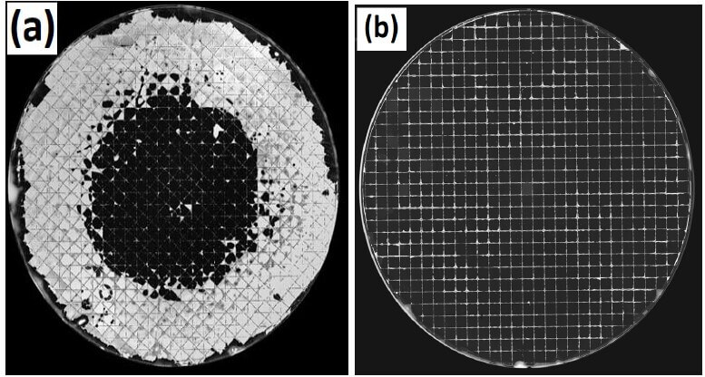
The top wafer of the bonded wafer pair could be thinned down from the original thickness of 775μm to 50μm thickness without any issues provided that the CMP process is well optimized and no bonding voids are observed in the C-SAM analysis.
Surface Cleaning
Commercial CMP tools have in-situ scrubber cleans to remove particles generated during the process. Defects are classified into four categories:
- Surface particles
- Embedded particles
- Residues
- Scratches
An additional external wet clean process step is required when the presence of residues and surface particles are confirmed. No wet clean process step is required for embedded particles and scratches since they cannot be removed. The associated risk with the additional wet clean process at this stage is that the incoming critical wafer surface conditions will be altered. If the critical parameters of the incoming wafers are already close to the above threshold values, then the wet-clean process time needs to be significantly reduced. Typically, it is the Cu Ra value, which is the most sensitive during post-CMP wet clean.
Post Bond Annealing
Post-bond annealing is required in hybrid bonding for proper Cu-Cu diffusion bonding to occur. The typical annealing temperature used for TEOS SiO2 is between 300°C-400°C. The minimum annealing time commonly being practiced is about 2h. Appropriate annealing temp is critical for achieving a void-free bond interface and it is directly linked to the Cu dishing value. If the annealing temperature is higher than optimum, it will result in microcrack formation in the dielectric region external to the Cu pads. An annealing temperature lower than what is desired will result in voids at the Cu/Cu interface since Cu mating surfaces will not come into contact and subsequent Cu diffusion bonding across the interface will not occur.

Pad Alignment
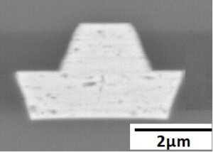
Both lithography and wafer bonding contribute to misalignment. The tool specification for the wafer bonder misalignment is ± 0.5μm. Through several SEM cross-sections of the dies from the same wafer, IME confirmed that misalignment varied between 0.5μm and 2.5μm for a Cu pad size of 3μm. Non-uniformity in misalignment can be resolved by the proper design of mating Cu bonding pads.
The Latest from Intel
Bloomberg reports that new Intel CEO, Pat Gelsinger, pledges to regain the company’s lead in chip manufacturing.
Gelsinger reportedly stated, “I am confident that the majority of our 2023 products will be manufactured internally…At the same time, given the breadth of our portfolio, it’s likely that we will expand our use of external foundries for certain technologies and products.”
This kind of statement clearly answered no one’s questions about what Intel’s future holds for them. Will they be offshoring 49% of their production? Will they be offshoring their advanced chip production to TSMC and/or Samsung?
Although he is also quoted as stating, “We’re interested in resuming that position as the unquestioned leader in process technology.” IFTLE would simply respond “Easier said than done.”
Gelsinger plans to provide more details after officially taking over the CEO role on Feb. 15 so I guess we will have to await more details then….
For all the latest in Advanced Packaging stay linked to IFTLE……………………………….


