SEMICON China attracts the world’s leading technology companies who design, develop, manufacture, and supply the technologies to manufacture the microelectronics that drive today’s most sophisticated consumer and commercial electronic products. Many of our 3D InCites community members are exhibiting and/or presenting during the show. Here is a preview of what to expect, March 17-19, 2021 in Shanghai, China.
SEMICON China 2021 Presentations:
Lam Research
Lam is a sponsor of SEMICON China 2021, as well as the sponsor of the Grand Opening Keynote. Tim Archer, president, and CEO, will help kick-off the event, sharing his thoughts on China’s critical role in driving growth in the semiconductor industry and his outlook on the opportunities ahead. In addition, Scott Meikle, senior vice president in Global Customer Operations, will join leaders throughout the industry in the Grand Opening Keynote, giving his perspective on the changing technological landscape and the company’s continued collaboration with partners to deliver breakthrough semiconductor advancements.
(Keynote) New Collaboration in the New Normal
Scott Meikle
Grand Opening Keynote
Wednesday, March 17, 3:05 PM
Concurrent with SEMICON China is the China Semiconductor Technology International Conference (CSTIC), one of the largest annual semiconductor technology conferences in China. Held on March 14-15 in Shanghai with a virtual forum through April 11, the conference will cover all aspects of semiconductor technology and manufacturing, including devices, design, lithography, integration, processes, emerging semiconductor technologies, and silicon material applications. You can find a summary of Lam’s participation throughout the conference here.
SPTS Technologies
SPTS will be presenting at the Power & Compound Semiconductor International Forum, at SEMICON China 2021, on March 19, 2021.
Michael Yi will be presenting Plasma Etch Processing for Both Power and Wide Bandgap RF End Markets at 10 am.
SPTS Technologies, a KLA company, designs, manufactures, sells, and supports etch, PVD, CVD, and MVD capital equipment, providing advanced wafer processing technologies and solutions for the semiconductor and microelectronics industry. End-market applications include micro-electromechanical systems (MEMS), advanced packaging, LED, high-speed RF device IC’s and power semiconductors.
SEMICON China 2021 Exhibitors
ASE Group, Booth #7474
ASE is involved in all stages of the semiconductor manufacturing process. Services from front-end engineering test and wafer probing, to package design, substrate design and manufacturing, packaging and test, module, board assembly, and test and distribution are fully integrated into a single supply chain.
New high-density advanced packaging (HDAP) enablement solutions stemming from ASE’s participation in the Siemens OSAT Alliance, are engineered to help mutual customers create and evaluate multiple complex integrated circuit (IC) package assemblies and interconnect scenarios in an easy-to-use, data-robust graphical environment prior to and during physical design implementation. The OSAT Alliance program is designed to drive faster adoption of new HDAP technologies like 2.5D, 3D IC, and fan-out wafer-level packaging (FOWLP) for next-generation IC designs.
Dr. KK Kuo, vice president, R&D Center ASE Group, will be presenting on Heterogeneous Integration and the Development of Fan-out Packaging at 2:45 pm in the Advanced Packaging forum at SEMICON China 2021 on Thursday, March 18.
Brewer Science, Booth #2721
Brewer Science develops and manufactures next-generation materials and processes that foster the technology needed for tomorrow. Since 1981, the company expanded its technology portfolio within advanced lithography, advanced packaging, and printed electronics to enable cutting-edge microdevices and unique monitoring systems for industrial, environmental, and air applications.
Runhui Huang, Xing-fu Zhong, Gu Xu, Boyu Zhang, Jakub Koza, Sean Simmons will be presenting their research, Development of planarizing spin-on carbon material for high-temperature processes.
Wenkai Cheng will be presenting their research, A Novel Multifunctional Single-Layer Adhesive Used for both Temporary Bonding and Mechanical Debonding in Wafer-Level Packaging Applications.
Find more information about Brewer’s SEMICON China 2021 presentations by viewing the abstracts here.
CyberOptics Corporation, Booth #1387, 1325
CyberOptics, a leading global developer and manufacturer of high-precision 3D sensing technology solutions, will feature the WX3000™ metrology and inspection system with Multi-Reflection Suppression™ (MRS™) sensor technology as well as demonstrate high-precision WaferSense® sensors for semiconductor tool setup and diagnostics.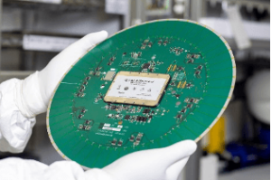
The NanoResolution MRS sensor integrated into CyberOptics’ WX3000 system provides sub-micrometer accuracy on features as small as 25µm. While retaining its ability to reject spurious multiple reflections, it adds the ability to capture and analyze specular reflections from shiny surfaces of solder balls, bumps, and pillars, allowing highly accurate inspection and 3D metrology of these critical packaging features.
The company also will digitally demonstrate high-precision sensors that process and equipment engineers use in the front-end of the fab to speed equipment qualification, shorten equipment maintenance cycles, lower equipment expenses and optimize preventative maintenance plans.
EV Group, Booth #2387
EV Group (EVG) is a leading supplier of equipment and process solutions for the manufacture of semiconductors, microelectromechanical systems (MEMS), compound semiconductors, power devices, and nanotechnology devices. Key products include wafer bonding, thin-wafer processing, lithography/nanoimprint lithography (NIL), and metrology equipment, as well as photoresist coaters, cleaners, and inspection systems.
Recently, the company announced plans to co-develop die-to-wafer hybrid bonding solutions for 3D-IC/heterogeneous integration applications. Hybrid bonding involving wafer-to-wafer as well as die-to-wafer integration is a necessary process step to support heterogeneous integration, a crucial component in extending Moore’s Law and enabling future generations of devices with increasing levels of performance.
EVG has invested significant resources to support this transition, including the establishment of its Heterogeneous Integration Competence Center™, which serves as an open-access innovation incubator for customers and partners to accelerate the development of new and differentiating heterogeneous integration products and solutions.
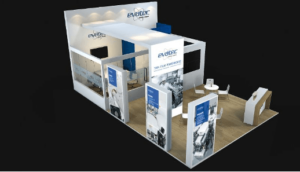
Evatec, Booth #3231
Evatec delivers complete thin-film production solutions for advanced packaging, power devices, MEMS, wireless technologies, and optoelectronics. Nominated for a 3D InCites Award, Evatec’s CLUSTERLINE® 200 platform, offers a solution for the deposition of next-generation AlScN piezoelectric materials enabling 5G or CLUSTERLINE® 300 for soft magnetic multilayers on 300 mm CMOS for power systems-on-chip applications.
 Within packaging applications like FOPLP and advanced IC substrate manufacturing the CLUSTERLINE® PNL platform is already production-proven. Advanced degas technology, and static panel processing during etch and deposition combined with the capability for handling larger panel sizes up to 650 x 650mm makes its second-generation platform the perfect choice for cost-effective volume production with the lowest particle count and best panel yield.
At 11:40 am, on Wednesday, March 17 during the New Technology Release Conference, Yuan Lu, technical marketing manager, Evatec China Ltd., will present Evatec Deposition Solution on 3rd Generation Semiconductor SiC-based Device.
ERS Electronic, GmbH, Booth #3711
ERS has been supplying innovative thermal test solutions to the semiconductor industry since 1970 and is famous for fast-ramping and precise low-noise thermal systems (-65°C to +300°C) for analytical, parametric, and wafer sort probing up to 300mm. The patented ERS flagship product for hot/cold wafer test, AC3(R), is available for package-level tri-temp applications for MEMS test.
ERS supplies the advanced wafer-level packaging market with its fully automatic debonders and warpage adjust tools used in the production of both 200mm and 300mm eWLB device packages. On a broader scale, ERS supports not only eWLB but many other fan-out wafer-level-package (FOWLP) technologies with its factory competence center that opened in March 2011.
Greater China Sales and Marketing Director Joshua Zhou will be at the booth to answer any questions related to the company’s thermal solutions for wafer probing and fan-out advanced packaging.
KLA, Booth #5721
KLA Corporation develops industry-leading equipment and services that enable innovation throughout the electronics industry, with advanced process control solutions for manufacturing wafers and reticles, integrated circuits, and packaging.
Visit the booth to learn more about KLA’s comprehensive portfolio of SensArray® products enabling in situ monitoring of process tools’ environments. With wired and wireless sensor wafers and reticles, an automation package and data analysis systems, SensArray products provide comprehensive information for a wide range of wafer and reticle processes. Wafer process equipment manufacturers, IC manufacturers and reticle manufacturers use SensArray data to visualize, diagnose and control process conditions.
LPKF, Booth #2579
As a leading provider of laser manufacturing solutions, LPKF Laser & Electronics helps to create more powerful electronic systems and increase functionality and efficiency for a broad range of applications and industries.
The LIDE technology (Laser Induced Deep Etching) developed by LPKF is a new enabling technology for a wide range of applications in microsystems technology. The needs of end customers and their business models are as varied as the applications. LPKF aims to offer all potential LIDE customers the easiest, barrier-free access to the technology so customers benefit from access to production service solutions as well as equipment solutions for selected applications and manufacturing environments.
SurplusGLOBAL, Booth #4645
SurplusGLOBAL, Inc., a global leader in the secondary equipment market, with over 1,500 pieces of equipment in its inventory. Its comprehensive inventory consists of more than one thousand 150mm, 200mm, and 300mm FAB, ATE, Package, SMT, and solar tools. The company has successfully provided solutions for the secondary semiconductor equipment market for over 14 years.
A new SurplusGLOBAL Cluster concept provides a one-stop solution of equipment, services, and parts in Yong-In, South Korea, offering access to the largest complex of used semiconductor equipment. Near 30 companies related to the semiconductor equipment industry are currently scheduled to move into the cluster. Plans are to complete the construction of the floor space 68,317 m2 (20,665 Pyeong) with six stories high by June 2021.
Trymax Semiconductor @AST’s Booth #N2431
Trymax delivers innovative plasma-based solutions for ashing, descum, surface preparation, isotropic etch, photoresist curing, and charge erase that are used in the fabrication of integrated circuits. Its NEO 2000 system for MEMS manufacturing is the latest photoresist removal equipment from Trymax and is the most flexible Plasma Ashing system for running critical low-temperature descum processes and high-temperature bulk photoresist strip processes. These steps are crucial for the manufacturing of high-performance accelerometers and gyroscopes used in consumer, automotive, and industrial applications.
The platform’s handling system can handle up to three different wafer sizes, ranging from 3- to 8-inch in diameter, and can be configured in a non-backside touching mode and in a dual side wafer processing. The motorized chamber lifting system makes it possible to handle wafers with double side coating for ashing both sides as well for handling Taiko wafer substrates. With the wide range chuck, it’s easy to switch full automatic from high to low temperature with the integrated chuck air-cooling loop.
Veeco, Booth #3719
Veeco designs, manufactures, and markets thin film process equipment that enables high-tech electronic device production and development all over the world.
Veeco’s proven metal-organic chemical vapor deposition (MOCVD), molecular beam epitaxy (MBE) lithography, laser spike annealing, ion beam, single wafer etch, and clean technologies play an integral role in producing LEDs for solid-state lighting and displays and in the fabrication of power electronics, photonics, optics, and advanced semiconductor devices. The company also offers solutions to the semiconductor wafer inspection market that leverages proprietary coherent gradient sensing (CGS) technology and provides atomic layer deposition (ALD) tools to leading research organizations.


