
The team at EV Group has done it again. They looked around at where the microelectronics industry is headed, identified a gap and set out to fill it. This time, the gap fell in between research and development (R&D) and the ramp to manufacturing for customer products built using heterogeneous integration technology. So, leveraging lessons learned from launching its NIL Photonics Competence Center six years ago, the company has established a first-of-its-kind, Heterogeneous Integration (HI) Competence Center.

According to a press release issued today by EVG, “the HI Competence Center combines EVG’s world-class wafer bonding, thin-wafer handling, and lithography products and expertise, as well as pilot-line production facilities and services at its state-of-the-art cleanroom facilities at EVG’s headquarters in Austria, supported by EVG’s worldwide network of process technology teams.” The goal is to help customers accelerate product development, minimize risk, and develop differentiating heterogeneous integration and advanced packaging technologies, all the while guaranteeing the highest IP protection standards of pre-release products.
I spoke with EVG’s Markus Wimplinger, corporate technology development & IP director, and Thomas Uhrmann, director of business development, to learn more about the motivation that fueled this project, and how it fits into EVG’s corporate culture.
A History of Heterogeneous Integration Technology and Collaboration
Remember the EMC3D Consortium launched by Semitool? Those were the early days of 3D through silicon via (TSV) development, and EVG was one of the founding members. Not only has the company spent the last 15 years or so honing its experience, knowledge and leading-edge wafer-level packaging processes, but they’ve also fostered a collaborative spirit along the way.
Moreover, they have believed for longer than most, that advanced packaging may hold the key to delivering highly innovative products.
“Our intention is to support our heterogeneous integration technology customers with our capabilities and expertise to help them bring new devices to life and leverage and differentiate products,” says Wimplinger, adding that one of the biggest challenges of packaging development is taking an idea from concept to final production. Part of the motivation, of course, is the mutually beneficial nature of the program. Supporting customers through development allows EVG to further strengthen its own capabilities.
Uhrmann noted that in the past, packaging a semiconductor device was a fairly straightforward process for OSATs. But the emergence of systems-in-package (SiPs) and heterogeneous integration has created a “huge playground for new concepts and devices. Adding the ‘secret sauce’ (aka packaging technology) makes it possible to customize concepts,” he explained. Moreover, the requirements for HI are changing. Many companies are now developing approaches in-house, and there is more involvement from OEM partners. “Companies are looking for services that provide new processing solutions.” He said. “Our innovative incubator approach provides a secure environment for our customer base. They can use our processes on new ideas and ramp them to production. We are investing to collaborate with our customers.”
Lessons Learned in Photonics Development
EVG’s experience for launching the HI Competence Center is not limited to its knowledge of heterogeneous integration technologies. In 2014, the team identified a similar gap in the company’s photonics customer base and established the NIL Photonics Competence Center, leveraging its nanoimprint capabilities including SmartNIL, lens molding, hot embossing/µ-Contact, and layer transfer processes. While EVG’s capabilities in heterogeneous integration are markedly different, the core concept of the competence center proved to be repeatable.
“We found a good blueprint that has worked for six years for photonics product development that includes engagements models and a systematic approach from feasibility to production,” added Uhrmann. Relying on this proven structure means all the protocols for documentation of the customer’s project are entered into an IP protected system. The same approach can be applied to HI.
How the HI Competence Center Works
“Heterogeneous integration involves a variety of different technologies, from silicon to compound semiconductors, MEMS, CMOS, optics, micro-optics, and traditional semiconductors,” said Wimplinger. “We are in a position to help customers integrate components into packages.”
Customer engagement can be as simple as partnering on a single process step, such as temporary bonding, to providing support for an end-to-end process flow all the way to technology transfer into the manufacturing environment. For the process steps that don’t fall into EVG’s core competencies, customers’ exclusive partners based on processes of record (PORs) are brought into the project.

“We are providing an incubator for an idea and promoting the process flow. How far it goes depends on the customer,” explained Wimplinger. Customers may come from different parts of the supply chain. For example, an OEM may be incubating ideas for the next product line, or manufacturing customers might be trying out a process block before tool purchase. “We decide together who the partners will be,” he added. “We need to be dynamic and flexible to enable customers to get the results and performance they desire.”
Bridging the Gap
Both Wimplinger and Uhrmann pointed out that the HI Competence Center is in synergy with R&D centers and manufacturing companies. R&D centers, in particular, offer unique skillsets for device development. When the customer comes to the HI Competence Center, they will have a product idea that’s supposed to work. The HI Competence Center is intended to work in the interface between R&D and manufacturing to provide a bridge from product idea to manufacturing, typically focusing on a more limited portion of the overall process flow than what an R&D center could provide.
“To my knowledge, what we are providing here is unique in the industry,” said Uhrmann. “This holds true both from the perspective on how we partner with our customers and other suppliers, as well as the specific capabilities that we can provide given our leading position in temporary and permanent wafer bonding and lithography.”
With all this investment in heterogeneous integration, I was surprised to discover that EV Group so far has not become an active member in the Heterogeneous Integration Roadmap. Uhrmann said they have been in close contact with different parties who are involved and have followed its activities closely, understanding that it’s an important part of the puzzle. Now that the first edition has been published, we will see more EVG participation, he said.
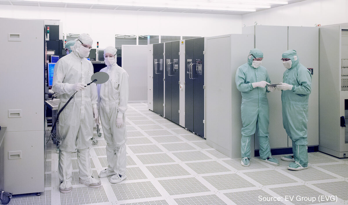
Housed in EV Group’s ever-expanding headquarters in Schärding, Austria, the HI Competence Center will be completely outfitted and ready to ramp by the middle of the year, said Wimplinger. Customer engagement is already well underway. Get more information here. ~ FvT


