
EVG S&R Mastering Shop™ further lowers barriers to adoption of nanoimprint lithography for wafer-level and panel-level production applications such as optical sensors, micro-lenses, nanophotonics and silicon photonics
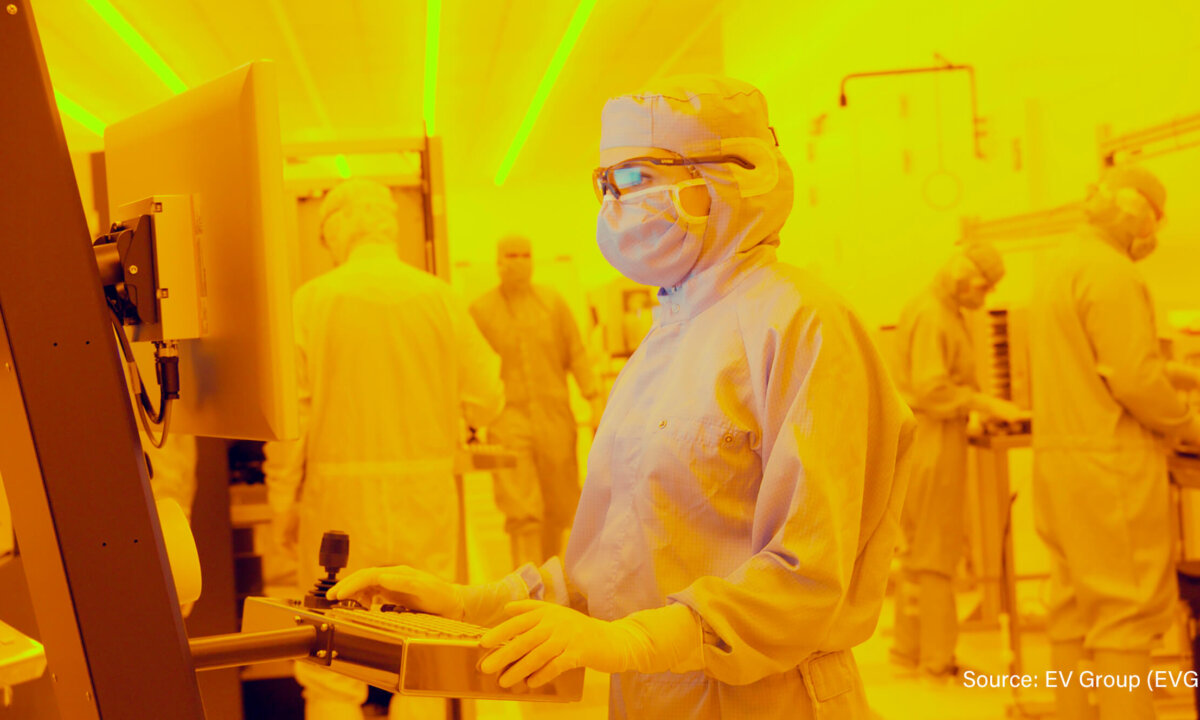
EV Group (EVG), a leading supplier of wafer bonding and lithography equipment for the MEMS, nanotechnology and semiconductor markets, today announced that it has established the EVG Step-and-Repeat (S&R) Mastering Shop, a new service offering to help customers accelerate the deployment of nanoimprint lithography (NIL) in high-volume manufacturing. The EVG S&R Mastering Shop™ uses EVG’s own equipment and cleanroom facilities to provide contract manufacturing of large-area master templates and stamps, which are used to produce working stamps for wafer-level and panel-level NIL processing.
By eliminating the capital costs associated with owning dedicated S&R systems for master stamp fabrication, customers can more easily integrate NIL technology in their new product designs. Devices and applications benefiting from EVG’s S&R NIL solutions include augmented reality waveguides, advanced micro-optics for optical sensors, micro-lenses, nanophotonics and silicon photonics. The EVG S&R Mastering Shop is a key addition to EVG’s NILPhotonics® Competence Center framework, located at EVG’s corporate headquarters in Austria.
Benefits of S&R NIL Mastering
Using S&R mastering, a large-area master stamp can be produced from a single-die “hard master”. This S&R master can then be used to replicate tens or hundreds of working stamps, which are used to imprint the functional structures on substrates. This replication method minimizes wear-out and risk of introducing defects to the expensive master. The ability to replicate larger master molds over ever-larger substrates – including 300-mm wafers, panel-sized substrates and inserts for roll-to-roll (R2R) manufacturing – allows more devices to be produced simultaneously as well as allows for the production scaling of larger individual devices without stitching. EVG is the only company to offer the complete breadth of products, services and expertise for S&R mastering and wafer-level NIL processing that enable rapid and cost-effective scaling of NIL-enabled products from R&D to high-volume production.
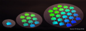
waveguide master courtesy of WaveOptics.
“EVG has pioneered the development and maturation of nanoimprint lithography with more than 20 years of experience in this innovative technology,” stated Markus Wimplinger, corporate technology development & IP director at EV Group. “This year marks even more developments in NIL for EVG. Earlier this month, for example, we introduced our next-generation EVG®770NT step-and-repeat NIL system, which paved the way for large-scale master stamp fabrication for NIL volume production applications. Now with our new S&R mastering services, EVG is eliminating even more barriers to NIL adoption for our customers by providing a one-stop shop for structured masters within a flexible and cost-effective service model. We are pleased to achieve yet another new NIL milestone by being the first company to offer S&R NIL mastering services for wafer-level and panel-level production applications.”
Details of EVG S&R Mastering Shop
EVG’s S&R solutions offer significant yield and cost advantages compared to conventional mastering methods, such as diamond drilling, laser direct writing and electron-beam writing, which are difficult to scale up to larger substrates due to their low throughput and high cost of implementation. Incorporating the S&R process enables the use of best-performing dies and the ability to efficiently bring these high-quality patterns into production lines.
As part of EVG’s new S&R mastering services offering, the company has added a new cleanroom area with dedicated S&R and metrology systems for contract services. The EVG S&R Mastering Shop utilizes EVG’s newly introduced EVG770 NT step-and-repeat NIL systems, which enable large-area master stamp fabrication on substrate sizes up to 300-mm wafers and Gen-2 (370mm x 470mm) panels with industry-leading overlay accuracy and resolution. All core infrastructure is located in an access-controlled environment and operated by a dedicated team to maintain protection of customer IP.
In addition to producing master stamps, EVG also offers the ability to produce working stamps and original hard masters for customers. Furthermore, within the framework of its NILPhotonics Competence Center, EVG also offers imprint process development, materials qualification and optimization, as well as device prototyping and pilot-line manufacturing – all with the highest levels of confidentiality and IP protection.

EVG®770 NT step-and-repeat NIL system.
Service Availability
The EVG S&R Mastering Shop is now open for servicing customers at EVG’s headquarters. For more information, visit https://www.evgroup.com/products/process-services/nilphotonics-competence-center.
EVG at SPIE Digital Optical Technologies and NIL Industrial Day
This week, EVG is presenting an invited paper on the benefits of NIL in manufacturing high refractive index waveguides at the SPIE Digital Optical Technologies Conference, being held online on June 21-25. In addition, EVG is presenting on S&R mastering at NIL Industrial Day, being held online on June 22-23.


