
The IEEE 3DIC Conference was held at North Carolina State University in Raleigh NC in person from Nov 15-18 2021. The Conference Chair was Paul Franzon. Let’s take a look at some of the key presentations.
CEA Leti – Copper Hybrid Bonding for GaN on Silicon
Dubarry of Leti presented “3D Interconnection Using Copper Hybrid Bonding for GaN on Silicon Wafer”
3D integration through-wafer stacking is obtained with a GaN-based wafer integrated on Si substrate and CMOS wafer. Wafer-to-wafer hybrid bonding technology was used with Cu patterns embedded in a silica matrix to provide direct 3D links in a face-to-face scheme with a pitch of 3 μm. Then, 1 μm Cu through silicon via (TSV)-last patterned through the SOI substrate of the CMOS wafer with AlCu routing lines was followed by copper pillars to connect the stack to the package (Figure 1).
The major challenge with this integration is the presence of III-V material (GaN). It is necessary to take into account that GaN and Si have a large mismatch of the in-plane thermal expansion coefficient (TEC) (5.59×10⁻⁶ K-1 for GaN and 2.6×10⁻⁶ K-1 for Si).
A copper damascene via level was patterned on top of the last metal level of mother wafers to provide electrical links at the required places. A specific planarization and contact strategy between the Cu damascene via layer and the AlCu CMOS metal level were carried out. A successive Cu damascene bonding level was achieved with the usual flat topography required for defect-free hybrid bonding purposes.
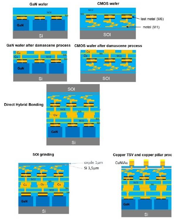
The copper damascene layer is fabricated by patterning 400°C plasma etched chemical vapor deposition (PECVD) tetraethyl orthosilicate (TEOS) silicon oxide. After oxide deposition, annealing is applied to eliminate any water molecules absorbed in the dielectric layer. Ti/TiN diffusion barrier layer and PVD copper seed layer dedicated to electrochemical deposition (ECD) copper growth provided copper metal layers. The most critical step is Cu /SiO2 planarization using chemical mechanical planarization (CMP).
Successful bonding needs a very low nano-topography, a copper roughness near 0.5 nm, and a Cu dishing value smaller than 5 nm to be compatible with direct bonding requirements. After CMP, both 200 mm top and bottom wafers were bonded with an EV Group Gemini system equipped with a specific alignment verification module (AVM). The top to bottom wafer alignment characterization was achieved by infrared (IR) transmission of the AVM.
Intel on Chiplets
Intel Fellow, Debendra Das Sharma, presented the opening plenary entitled Future Challenges for On Package Interconnect. Das Sharma, like others, pointed out that Gordon Moore, the golden boy of on-chip integration in 1965, also stated that at some point “…it may prove to be more economical to build large systems out of smaller functions which are separately packaged and interconnected”.
It is clear that they are giving him credit for predicting the current era that IFTLE calls “disintegration” and others call “disaggregation”. To me, since we all agree we have been “integrating” on-chip for several decades, the current trend to create separate chiplets for smaller functions must be “disintegration” but for some reason, others avoid the term like it is politically incorrect. In any case it is simply semantics……
Das Sharma lists the following reasons for using chiplets:
- Reticle size limit, yield optimization, scalable performance
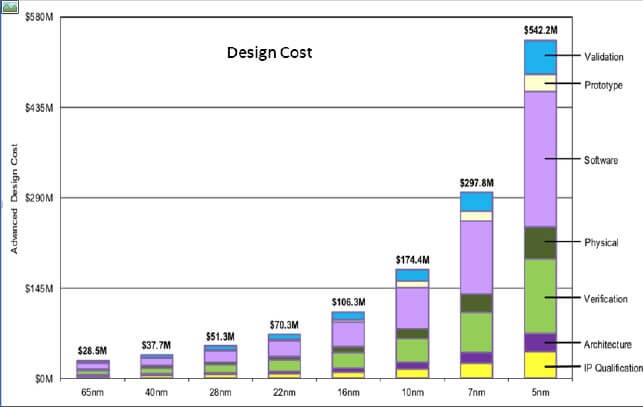
- Increasing design costs at leading-edge process nodes (see below)
- Use latest nodes only for required advanced functionality, not the whole chip
- Different process nodes optimized for different functions (memory, logic, co-packaged optics)
- Quicker time to market since reusing qualified IP for some functions
- High power-efficient bandwidth with low-latency access
He outlined key challenges as:

- Technology choices: different usages/segments – challenging for common silicon
- Power delivery and cooling
- Repair strategy to minimize failure and optimize yield
- Debug – controllability and observability
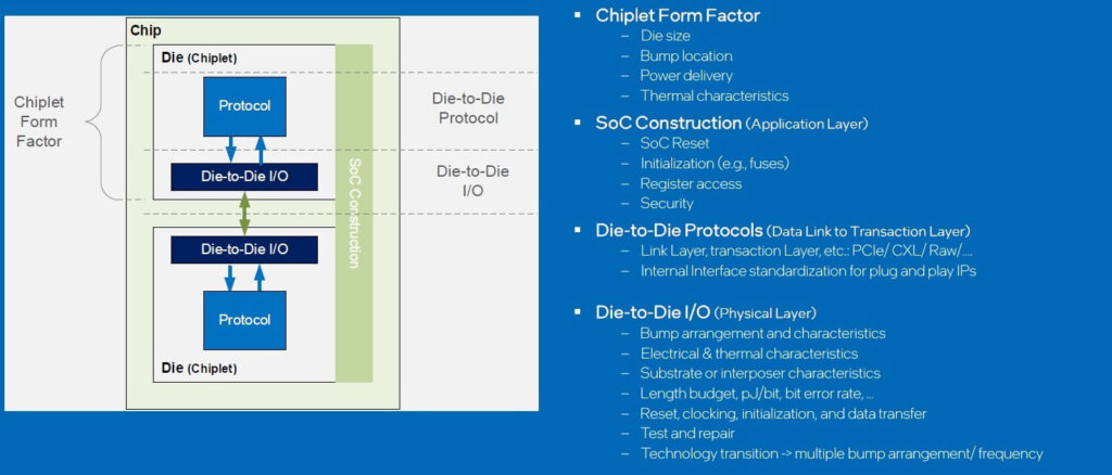
He agrees with most of the community that die-to-die standardization will be essential to developing an open ecosystem. This will include chiplet form factor, chiplet construction, die-to-die I/O and die-to-die comm protocols as shown in Figure 3.
Bond Strength Optimization of Plasma-activated, Low-Temperature Oxide-oxide Fusion Bonding through Thermocycling.
Kruger of IHP – Leibniz discussed his studies on the influence of annealing time and the number of annealing steps on the shear strength of plasma-activated low-temperature oxide-oxide fusion bonding wafer stacks. A two-step-annealing process, with the first annealing step between 2-6 hours, and the second annealing step of 20 min or less, results in a shear strength increase of an order of magnitude compared to a single annealing step with equal or longer annealing time.
3D for More than Moore
Mustafa Badaroglu of Qualcomm discussed 3D for More than Moore.
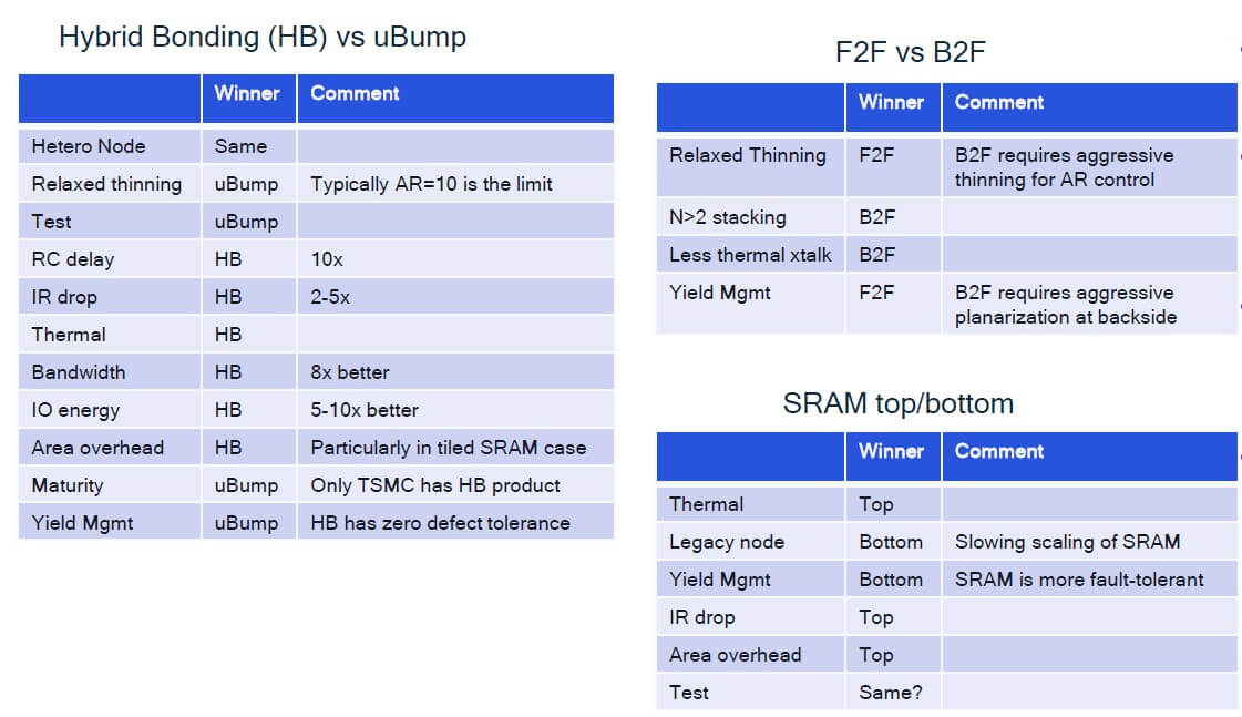
Buried in the presentation was this interesting chart on the pros and cons of various 3D fine-pitch stacking options (Figure 4)
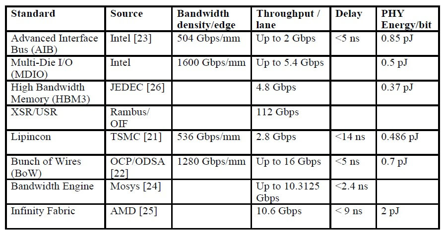
The table shown below compares chiplet communication protocols (references can be found in the original presentation).
For all the latest in Advanced Packaging stay linked to IFTLE………………


