“How is heterogeneous 3D integration defined?” There are certainly different understandings in the microelectronics community regarding the definition of heterogenous...
As traditional semiconductor scaling becomes increasingly complex and cost-prohibitive, transitioning from planar chip packaging architectures to 2.5D/3D stacked die package...
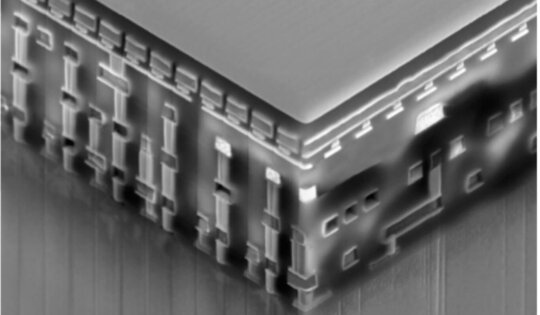
A novel copper interconnection technology is being pioneered by Georgia Tech’s Packaging Research Center (GT-PRC) to achieve manufacturable solder-free assembly at...
Moore’s law is approaching physical limitations of CMOS scaling, and three dimensional (3D) integration technologies have been proposed as solutions....
Microelectronic products all have mechanical, thermal and electrical properties that degrade until the device is permanently damaged. Path finding adds...