

A novel copper interconnection technology is being pioneered by Georgia Tech’s Packaging Research Center (GT-PRC) to achieve manufacturable solder-free assembly at low temperatures. By interfacing engineering and process design, the Cu interconnections are shown to meet both thermal cycling and ultra-high current-handling needs. This technology is now being applied to mobile and high-performance computing with ultra-high I/O density down to 20µm pitch, along with embedded power and RF modules for meeting the current-handling and height requirements. GT-PRC is now commercializing this technology with its industry partners.
System Scaling with Highly-integrated 2.5D and 3D Glass Interposers and Packages
Emerging smart systems require a new system scaling strategy with ultra-thin devices and system components that have the shortest wiring and interconnections. This system scaling starts with a low-cost, low-CTE, high-stiffness 3D interposer that provides chip-to-chip interconnects at back-end-of-line (BEOL) pitch for ultra-high I/O density with short interconnect length to reduce latency and footprint, and enable high bandwidth at low power. The interposers are manufactured with panel-based processes with semiconductor ground rules at much lower cost.
Glass is envisioned as the next generation platform material for this highly-integrated 3D interposer vision. It is a superior alternative to silicon and organic interposers because of its outstanding electrical resistivity and ultra-low electrical loss for high-frequency RF applications, as well as its availability to form low-cost, ultra-thin interposers from large-area processing¹⁻².
Low-temperature Ultra-short Interconnections with Ultra-high I/O Density
Seamless integration of chip-to-chip interfaces for high bandwidth of 1TB/s at low power is the main objective of 3D interposers. The need for such bandwidth in both mobile and high-performance systems is expected to drive off-chip interconnections pitch down to 10µm and below by 2020.³ This trend is described in Figure 1.
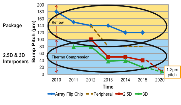
Reduction in pitch also leads to scaling down of standoff height and diameter of the micro-bumps. As shown in the top part of Figure 1, traditional solders cannot be scaled down to the targeted interconnection pitches because of their process limitations and inferior properties, higher risk of bridging at finer pitch, increased interfacial stresses due to reduced solder volume requiring careful control of intermetallics formation and growth, and poor current-handling capability.
Solder-free direct Cu-Cu bonding technologies for both wafer-to-wafer and die-to-wafer applications are emerging to address these challenges.⁴⁻⁵ However, these approaches necessitate bonding temperatures as high as 350°C, increasing package warpage and thus penalizing board-level reliability. The yield and throughput of Cu-Cu interconnections at ultra-fine pitch is also degraded by the necessity of high pressure in thermocompression bonding to accommodate non-coplanarities, costly additional process steps for surface treatment, roughness of bumps, and wafer and substrate warpage. Current proposed approaches are not compatible with existing infrastructures, tools and processes applied in high-volume manufacturing (HVM).
GT-PRC has pioneered a novel copper-based chip-level interconnection technology without solder, with the following attributes:
- Assembly at temperatures as low as 160℃
- Ultra-short interconnections (<10µm) for enhanced electrical performance
- Process tolerance to non-coplanarities of bumps and substrate warpage
- High-throughput manufacturable assembly processes compatible with current industry tools and processes applied in high-volume manufacturing
- Enhanced reliability
- Improved power handling – all at I/O pitches down to 50µm with organic interposers, and 20µm with glass and silicon substrates.
The low-temperature copper interconnection technology recently patented by the Georgia Tech 3D Systems Packaging Research Center⁶ comprehensively addresses the previous challenges with direct Cu-Cu bonding by these innovations:
- Prevention of copper oxidation by standard electroless Ni – immersion Au (ENIG) or electroless Ni – electroless Pd – immersion Au (ENEPIG) surface finish, applied on micro-bumps and pads.
- Accommodation of micro-bump and pad non-coplanarities by collapse of the interconnects under pressure during thermocompression bonding.
- Substrate warpage reduction with assembly at temperatures below the glass transition temperature Tg of certain low coefficient of thermal expansion (CTE ) laminates.
- Bumping cost reduction by eliminating solder plating and using ultra-short all copper bumps, about 10µm in height.
The schematic illustration of the interconnections is shown in Fig. 2.
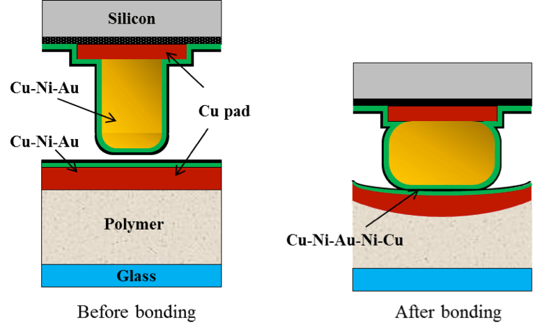
A polymer material with a filler-free composition such as pre-applied underfill (PAU) or non-conductive film (NCF) is first dispensed on the substrate bonding area with a fine control of the viscosity and deposited volume. B-stageable no-flow underfill (BNUF from Namics Corporation) was used for this set of experiments. After dispensing, this epoxy-based material requires B-staging at 70°C for 1hour in air. The Si die is then assembled onto the polymer-coated substrate by thermocompression bonding at 160°C, 365 MPa with a 10s dwell time at peak temperature, The BNUF material reaches a low-viscosity point at temperatures ~110-130°C, allowing the excess material to be squeezed out from the bonding interface and flow, enabling contact between Cu micro-bumps and pads, then starts hardening at higher temperature.
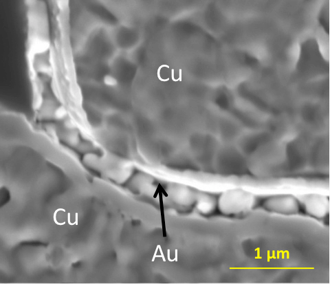
The cross-sectional SEM image of Cu interconnection after ion milling is shown in Figure 3. The top side shows the Cu bump on the silicon die, and the bottom side shows the Cu landing pad on the polymer dielectric on the glass interposer. Both the Cu bump and the Cu pad were plastically deformed under thermocompression. The 10µm-thick polymer lying under the Cu pad has sub-GPa modulus and therefore undergoes continuous viscoelastic deformation at the bonding temperature, leading to significant pad-deflection as well as bump-collapse. During thermocompression bonding, local metallic contacts are formed at the bonding interface.⁷ The surrounding underfill polymer further enhances the bonding strength of the joint and thermomechanical reliability performance. Metallic bonding happens due to plastic deformation first, and then and by solid-state diffusion at the bonding interfaces.

.
High-throughput Die-to-panel Assembly Demonstration
For either traditional flip-chip bonding or low-pressure thermo-compression Cu pillar with solder cap technology, assembly in industry-standard low- to high-volume lines is usually performed on a substrate strip to facilitate BGA balling for board-level interconnection. Two assembly strategies have been considered for manufacturable solder-free copper interconnections:
- Tacking the die by pre-cure of a non-conductive polymer (underfill, NCF, NCP, ACF, NCA, ACA) followed by gang bonding where pressure is applied on multiple dies at once to reflow the solder and fully cure the polymer material.
- Bonding of each die individually using a thermocompression tool, potentially followed by a batch-type process to cure the polymer.
Although the first scenario could potentially have higher throughput, it is more difficult to implement as it requires pressure uniformity on a strip-scale, which can only be achieved with high-accuracy equipment with micron-scale parallelism between the press plates. The second approach involves a specific assembly sequence where the heat transfer is dominated by the thermocompression flip-chip tool. The plate onto which the substrate is placed is maintained at a constant low temperature to limit substrate warpage and to prevent any degradation of the joints of the mounted components during subsequent assemblies.
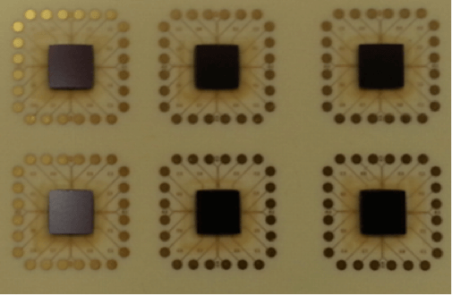
A panel-level process was developed using a Finetech Matrix semi-automatic flip-chip bonder with a placement accuracy of 3µm and controllable temperature and force profiles. The stage can accommodate a large substrate size as illustrated in Figure 4, and has thus a very low heat capacity with a temperature ramp rate limited to 6°C/s. A customized 6mm x 6mm vacuum-locked spring gimbal tool head, enabling pre-leveling of the die, was used to prevent any die tilt during assembly. BNUF was first dispensed on a substrate that can accommodate 15 dies, and B-staged. The substrate was then placed onto the stage and maintained at 70°C during the entire assembly sequence to slightly decrease BNUF viscosity and prevent misalignment of the die during placement. Each die is eventually picked, placed and bonded at 230°C applied for 3s. After assembly of all dies, the panel is subjected to an oven cure at 165°C for 3h in air to ensure that the BNUF material would reach its final solid stage, in order to achieve the high through-put die-to-panel assembly process.⁸
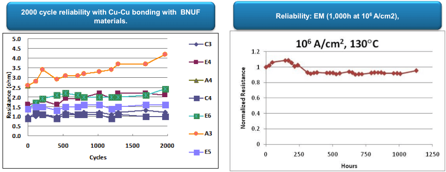
Reliability Characterization The superior thermo-mechanical reliability and electro-migration resistance at 106 A/cm² of these advanced copper interconnections were demonstrated on low-CTE organic and packages at pitches as low as 30µm.⁹⁻¹⁰ The results are summarized in Figure 5.
Summary
A novel low-temperature, ultra-fast, die-to-panel Cu interconnection and assembly process, compatible with standard thermocompression bonding tools was demonstrated by GT-PRC. Interface characterization indicated that the targeted metallurgical bond could be formed in a mere few seconds. A panel-level assembly sequence was developed and demonstrated with heat- transfer from the die -side exclusively. These preliminary results demonstrate a promising proof-of-concept towards industry-compatibility of Georgia Tech PRC patented technology. GT-PRC is now commercializing this technology as a compelling solution for the next-generation of ultra-fine pitch high-performance systems, starting a new era without solders.
Authors
P M Raj, Vanessa Smet, Tao Wang, Venky Sundaram, Makoto Kobayashi and Rao Tummala, 3D Systems Packaging Research Center, Georgia Institute of Technology, Atlanta, GA 30332-0560
References
- ‘Low-Cost Thin Glass Interposers as a Superior Alternative to Silicon and Organic Interposers for Packaging of 3-D ICs’ V. Sukumaran, Qiao Chen, Venky Sundaram and Rao Tummala, IEEE Transactions on Components, Packaging and Manufacturing Technology, Vol. 2, pp. 1426-1433, 2012.
- Tummala, R.R., 2.5 D Interposers – Organics Vs silicon Vs Glass, Chip Scale Review, July-August 2013, pp. 18-19.
- A. Sitaram, “Scaling 2.5D/3D: the Next R&D Challenge,” in 2nd Annual IEEE Global Interposer Technology Workshop, Atlanta, GA, Nov 14-16, 2012.
- B. Swinnen, W. Ruythooren, and P. De Moor et al., “3D integration by Cu-Cu Thermo-compression Bonding of Extremely Thinned Bulk-Si Die Containing 10μm pitch Through-Si Vias,” in Proc. Electron Device Meeting. International (IEDM), Dec 11-13, 2006, pp. 1-4.
- A. Fan, A. Rahman, and R. Reif, “Copper Wafer Bonding” Electrochemical and Solid-State Letters, 2(10), pp. 534-536, 1999.
- N. Kumbhat, A. Choudhury, V. V. Sundaram, R. R. Tummala, “Interconnect Assemblies and Methods of Making and Using Same”, US Patent # 8,633,601
- Tao Wang, Vanessa Smet, Makoto Kobayashi+, Venky Sundaram, P Markondeya Raj, and Rao Tummala, Modeling, Design, and Demonstration of Low-temperature Cu Interconnections to Ultra-thin Glass Interposers at 20 µm Pitch, Proceedings Electronic Components and Technology Conference, ECTC 2014.
- Vanessa Smet, Makoto Kobayashi, Tao Wang, Pulugurtha Markondeya Raj, and Rao Tummala, A New Era in Manufacturable, Low-Temperature and Ultra-Fine Pitch Cu Interconnections and Assembly Without Solders, Proceedings Electronic Components and Technology Conference, ECTC 2014.
- N. Kumbhat, A. Choudhury, and G. Mehrotra et al., “Highly Reliable and Manufacturable Ultra-fine Pitch Cu-Cu Interconnections for Chip-last Embedding with Chip-first Benefits,” IEEE Trans. CPMT, Vol. 2, No. 9, pp. 1434-1441, Sept. 2012.
- Sadia A. Khan, Abhishek Choudhury, Nitesh Kumbhat, P. Markondeya Raj, Venky Sundaram, Georg Meyer-Berg, and Rao Tummala, Multi-Chip Embedding Technology Using Fine Pitch Cu-Cu Interconnections, Transactions on Components, Packaging and Manufacturing Technology. Issue 2, Feb. 2013, pp. 197-204.


Markondeya ( ex KGP ) :
Looks promising. Some concerns about opens due to non co-planarity, the effect of deformation of the 10 um thick polymer layer on substrate on underlying metallization / vias. Any limits on die size / yield, max. no of bumps / pitch, bump pad on via etc. due to these concerns ? Would be interesting to find out more as your work progresses.
For reduction of bumping cost you / Rao may revisit our paper in ECTC 2004 for low-cost electroless Ni column bumps.
best
Dev ( ex KGP )