
I have to admit, for some time I’ve been fairly skeptical about glass interposer technology as a viable alternative to silicon interposers. It’s not that I doubted the expertise of research scientists like Rao Tummala and Venky Sundaram at Georgia Tech’s 3D Packaging Research Center (PRC), who have been evangelizing about the low cost and performance benefits of glass over silicon for a number of years. Its that I weighed it against the expertise of Madhavan Swaminathan, of E-System Design, and also Georgia Tech’s PRC,who enumerated the limitations of glass such as impedance issues and lack of thermal conductivity; and the cost benefits only being substantial if glass interposers are manufactured in panel form, rather than wafer. Additionally, every time the manufacturability of glass interposers came up during industry event panel discussions, the lack of a manufacturing infrastructure was pointed out by manufacturing companies.
But now I’m told a louder voice is clamoring for the development of a panelized glass infrastructure for the manufacture of low-cost glass interposers. The voice is so loud that glass substrate and tool suppliers are leaping into action to put the required infrastructure into place. Only one person was willing to reveal the industry heavy hitter to me, and I promised to keep it to myself. Just knowing it was enough to make me take the glass interposer movement seriously. I spoke to a number of suppliers exhibiting in the ECTC 2014 technology corner. There are still varying views on glass interposers as an alternative to Si; but there were clearly more on the pro-glass side than there used to be.
 Klaus Ruhmer, director of lithography sales, Rudolph Technologies, was the first to bring this shift in support for glass interposers to my attention as he demonstrated the company’s new JetStep S-Series lithography stepper for interposers. “Interposers, in our opinion, should be made in panels, not wafers, to achieve economies of scale,” he explained. “An interposer is a ‘dumb’ device and it needs to be cheap and manufactured in large scale.”
Trying to poke holes in his argument for glass, I started in on the limitations:
What about the lack of infrastructure? It’s great that Rudolph has a litho tool, but that’s not quite a whole line of tools. Ruhmer’s response: the tools exist for the rest of the processes, he told me. Tools for sputtering, metallization, lithography, etc. – all exist for manufacturing flat panel displays. Additionally the substrate industry can accommodate panels.
I checked in with a number of other tool vendors in the technology corner who supply the semiconductor industry to get their take on the feasibility of providing tools to accommodate glass panels. Laura Mauer, CTO, SSEC, says its possible to spin or spray coat panels by putting a round frame around the panels. Their coat/bake chambers can be configured for flat panel display manufacturing.
SPTS’s Keith Buchanan told me that although he’s yet to see a convincing argument on how address thermal issues for glass, and that Si still has an advantage, he says there are compelling arguments for it in terms of RF. He also said he sees no inherent issues with performing CVD sputtering processes on panels. With thin glass, he said the panels still need to be bonded to a carrier, and require room-temperature CVD passivation. Additionally, stress-tuning capabilities are a must. He predicts that Si will be first to the market, with a “gentle pulling” 5 or six years out for glass interposers.
 In the course of answering my questions about the Nova Plus Die Bonder, Amicra’s Managing Director, Johann Weinhaendler, Ph.D, explained that while the current high volume manufacturing application space for this thermocompression die bonder is fan-out wafer level packaging, it was designed for 450mm wafers and panels, and could conceivably accommodate die-to-die or die-to-panel assembly on glass panels for interposer technologies. The tool reportedly achieves 2.5µm accuracy in under 3 seconds; achieving 1200 UPH, is cleanroom class 10 capable, and has been field approved by customers for 3D packaging applications.
(During my recent tour of Oerlikon Systems applications lab in Balzers Lichtenstein, I saw a SOLARIS S380 — a version of the company’s SOLARIS PVD system developed for antireflective and contact material deposition for photovoltaic cells, as well as touch panel displays — being configured to handle larger substrate sizes. At the time I did not think to ask about panelized processes for glass panels, but it wouldn’t be a huge leap, would it?)
Ok. So the tools exist. Who’s going to invest CapEx to put in a panel line for glass interposers? The OSATS? They’ve just all invested heavily in 300mm wafer lines for backside processes for 2.5D and 3D IC technologies. Ruhmer speculated that it might be existing substrate companies, who would need to accommodate the smaller feature sizes of glass interposers. Perhaps the OSATS who are manufacturing fan-out wafer level packages. Some have already announced panel capabilities for FOWLP. Would it be a huge leap to add capacity for manufacturing glass interposers?
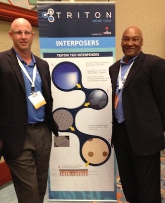 Or perhaps it will be dedicated interposer manufacturers, like Triton Microtechnologies, who have already been manufacturing glass interposer wafers for over a year. Tim Mobley, CEO of Triton, told me the company is actually equipped for glass panels, because its possible to retrofit those tools to handle wafer formats, but not possible to go in the other direction. Therefore, they cut the wafers out of glass panels because the glass is cheap. That way they can supply them to the wafer world for the remaining process steps.

Mobley, a former Ratheon engineer with expertise in the RF field, agreed with Ruhmer that lessons learned from flat panel display and the solar market transfer directly to what’s needed for glass, and that a glass interposer infrastructure is possible. These lessons extend to figuring out how to metallize glass to create the interposers, and do finer pitch features.
“The solutions are available. It’s a new application for existing manufacturing technology. The wafer world just isn’t used to it,” said Ruhmer. “Rudolph is already a supplier to the panel world. It’s not about marketing a new tool line. It’s about marketing a new business model.”
Not surprisingly, Corning is thrilled with this newfound support for glass. They’ve invested heavily in R&D, partnering with institutes like RTI and ITRI, to address the challenges of glass – namely thermal conductivity and impedance issues. “Two years ago there was talk about impedance issues and the thermal limitations of glass,” said Aric Shorey, PhD, Sr. technical manager, semiconductor glass wafers, Corning. “But people are learning to design with glass, and can design out impedance issues.”
Additionally, Shorey says that the thermal argument is used to discount glass, but there’s actually more to the story. The company co-authored and presented a paper at ECTC 2014 with ITRI showing thermal data using glass interposers. “There are plenty of solutions out there to handle thermal issues,” he said. “In some cases its an advantage. Glass can isolate devices from the heat.”
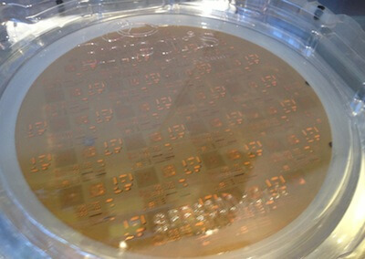
Corning is now supplying glass in wafer and panel format with vias already in it. On display in its booth is the first ever 300mm glass interposer with through glass vias (TGV) developed in collaboration with ITRI. Shorey says the company has achieved 25µm diameter holes, and with smaller diameters on its roadmap. He says glass is dimensionally rigid, which gives it an advantage over organic laminates when it comes to accommodating finer features. He also noted that putting circuitry on glass is not an issue; it’s done with LCDs all the time.
Dean Malta, technical manager at the Center for Materials and Electronics Technologies at RTI International, said RTI has been working with Corning to develop Cu via filling and overburden removal processes for glass interposers. He said the via profiles of Si and glass are different. TSVs are vertical and subject to scalloping due to the deep reactive ion etch (DRIE) process. Through GLass Vias (TSVs) are laser-drilled and are tapered. Malta explained that they are easier to fill and require only a seed layer for plating. A barrier layer is not required because the glass interposers are passive, are more forgiving, and the via separation is good enough to accommodate Cu. Cu diffusion is only an issue when dealing with active CMOS Si, said Malta.
From what I can tell, nobody really thinks that it’s going to come down to a race or choice between Si and glass. The belief is that glass interposers will provide a low-cost solution for passive interposers; which is critical if we ever want to see 2.5D interposer solutions in consumer electronics. Si will still be required for “smart” interposer technologies that are in development for higher end applications. “There’s room for everybody,” said Shorey, “Its not going to be either/or; there are plenty of people who think glass interposers are a good idea.” ~ F.v.T.


