
The ECTC 2013 stats are in. This year showed increases across the board with:
- Over 1,300 attendees, the highest attendance ever, from 26 countries
- 377 technical papers, presented in 36 oral and five interactive presentation sessions, including a student poster session
- 12 sessions focused on 3D/TSV, including several of the best attended sessions of the conference
- 16 professional development courses attended by over 300 participants
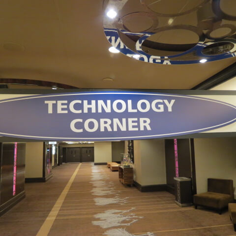
- 95 Technology Corner exhibitors – also a new record! (92 exhibitors already re-signed for next year)
While not all 95 exhibitors were 2.5D and 3D/TSV focused, I touched base with a number of those who are, and in addition to interviews with companies introducing unique 2.5D and 3D IC capabilities (SSEC, SPTS, Dow Corning, Multitest), I also met with a few exhibitors about updates to their 2.5D and 3D-related offerings. Here’s what they had to say.
Glass Interposers
 Triton Microtech got some traction introducing its through glass via (TGV) interposer technology at IMAPS DPC 2013 in March. The Tucson-based company is a subsidiary of Asahi Glass Co., Ltd. (AGC) and nMode Solutions Inc., and has started manufacturing glass interposers at it’s facility in Carlsbad CA, using AGC’s carrier-glass technology and via-hole drilling methodologies.
According to CEO, Tim Mobley, the via drilling technology results in coarse-pitch vias that can achieve over 3000 I/Os per processor. This is suitable for 2.5D applications, but not fine enough pitch for 3D IC. Currently, they are in the prototype-phase with most customers, manufacturing interposer wafers for 2.5D applications such as MEMS, RF, and optics – basically any thing with a need for transparency. The interposers are being manufactured on equipment similar to that of the solar industry using established techniques.
In response to a question about the controversy over a lack of infrastructure to support glass interposers, Mobley said the company took “a leap of faith” and decided to start the manufacturing process and create a supply chain. He says there’s lots of interest because of the “push back from silicon.” People use silicon out of convenience because the silicon infrastructure is in place. But silicon has drawbacks like leakage and reliability. LCD manufacturing technology can compete on the cost with silicon wafers, explained Mobley. I suspect we’ll be hearing more from Triton as glass interposers gain in popularity.
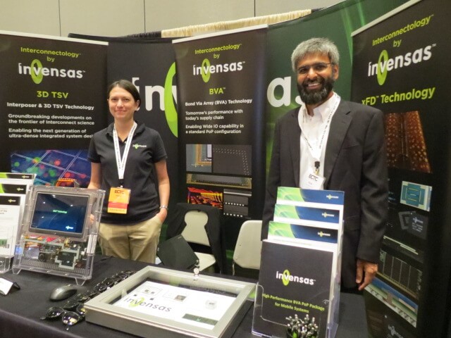 BVA Package on Package
Last year at ECTC 2012, Invensas launched its bond via array package-on-package (BVA POP) technology. This high-density logic on memory interface is based on wire bond technology, and has 432 I/Os on a 14mm x 14mm package size.
I caught up with Ilyas Mohammed, Invensas, who this year was presenting a paper on the second prototype BVA PoP that totals 1020 I/Os, for a substantial increase in logic/memory bandwidth. “We have done lots of process development to prove out manufacturing issues, ensuring 1000 plus wire bonds are all straight and that none are missing or bent, and how to inspect it,” reported Mohammed. He added that throughout the assembly process, the company has been working with wire bond equipment supplier, Kulicke & Soffa, to prove manufacturablity. They build small volumes in the labs, and large volumes at K&S.
Mohammed says they have addressed such issues in stacking 1020-pin BGA at very fine pitch on a logic package that has 20,000 pins sticking up. They worked with an assembly house to do PoP stacking, and have demonstrated high yields internally and at the OSAT (more than 99%).
The plan for the next few months is to address the test issue; testing the bottom logic package with interfaces on the top. This is new to the test industry due to the fine pitch (,3mm pitch on a o.24mm prototype), says Mohammed. Invensas is working in collaboration with test companies to address this. The current status of the BVA technology: 432 is fully qualified. BVA 1020 is assembled and going through qualification. Mohammed says he expects the BVA-1020 to be fully qualified in four months, with a test solution by the end of the year for both package versions.

On the 2.5D/3D IC front, Mohammed was able to provide some general information about the company’s progress with its 2.5D interposer test vehicle. The device is a silicon interposer with 2 micro-bumped die connected to it with 20µm x 100 µm pitch TSVs. 40µm pitch microbumps with copper posts attach the interposer to an organic substrate. The device is targeting “typical mainstream applications” such as a CPU next to a memory die, or stacked memory. I expect to learn more about this technology in the near future and will update readers on its progress.
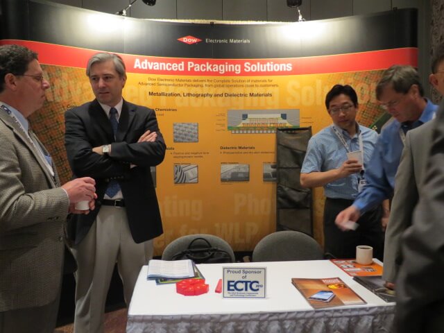 3D IC Materials
Lastly, I had a brief chat with Rob Kavanaugh of Dow Electronic Materials, who updated me on progress with the company’s 3D IC offerings since we last spoke at IMAPS Device Packaging Conference when I reported on the company’s temporary bond/debond solution.
Also at IMAPS DPC, the company presented on its current commercial offerings for SnAg capped Cu pillars: INTERVIA™ 8540 Cu Pillar and SOLDERON™ BP TS4000 SnAg, as well as reporting development of a a new XP Formulation A Cu Pillar that satisfies all key design criteria including highly uniform Cu Pillars (WID < 5%); a flat pillar profile (TIR<5%); smooth surface morphology; and compatibility with SnAg capping. Customer needs for finer geometries are driving further development work on next generation Cu Pillar and SnAg chemistries.
According to Kavanaugh, since IMAPS DPC, the company has been demonstrating its SnAg chemistry at higher speeds in capping applications, resulting in in less metal on the pillar for improved throughput and lower cost of ownership. Improvements in the die/bump morphology have resulted in more uniform bumps. Now that baseline materials for copper have been established, Kavanaugh says development focus now is to nail down the tin-silver chemistry to get it ready for manufacturing by ensuring that what was developed in the research phase is holding up in development with the customer. To this end, the company is engaging in selective demos in Asia. “I’m confident these demos will go well. We already have customer wafers plated in our labs with positive results,” said Kavanaugh.
And that’s a wrap, from ECTC 2013. Hope to see you next year!


