
A few weeks ago I spoke with SPTS’s David Butler, after he participated in the SEMICON Singapore 3D IC panel. We talked a lot about the importance of wafer planarity for performing backside processes like TSV reveal. Butler commented that regardless of a tool’s calibrated precision, its only as good as the wafer planarity. Last week at ECTC 2013, Butler’s colleague, Keith Buchanan, continued the story of the importance of maintaining flatness beyond the wafer thinning steps all the way through final assembly to ensure reliability and yields. He presented a paper titled Dielectric Stack Engineering for Via-Reveal Passivation, which explains the importance of passivation to provide wafer support prior to redistribution layer (RDL) and bumping, reduce stress, and prevent wafer bowing during the final assembly steps. Here are the key take-aways from that talk.
What SPTS offers, explained Buchanan, is a low-temperature plasma enhanced chemical vapor deposition (PECVD) process for via reveal passivation. “Low Temp” being the operative word, as conventional CMOS front-end PECVD processes used are at higher temperature, which isn’t compatible with temporarily bonded wafers.
Here’s how its done: after copper TSVs are exposed during the via reveal etch process, PECVD is used to deposit a silicon nitride/silicon oxide “stack.” This provides mechanical support for vias, and good electrical isolation from overlying RDL before bumping. (In this scenario we’re assuming dry etch reveal processes are being used, not a wet etch approach).
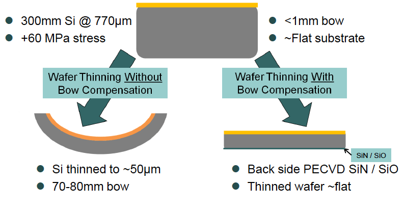
“We’re talking about wafers that are 300mm wide and have been thinned to 50µm thickness while attached to a carrier wafer,” explained Buchanan. “If we don’t manage the stress properly, when debonded, the wafer will curl up.” He added that in addition to support and isolation, PE CVD provides bow compensation. It matches the bow on the front side of the wafer with that of the back side, that when debonded, results in a completely flat wafer (Figure 1).
“Mechanical bow compensation at less then 200°C is incredibly challenging,” explained Buchanan. “SPTS’s unique PE CVD process guarantees stable films.” For example, they won’t absorb water when exposed to atmosphere.

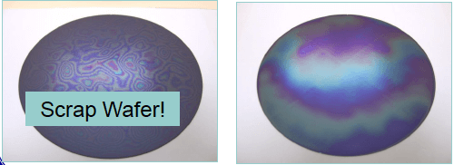
Accomplishing this required tool adaptation that allows for maintaining low temperatures, process adaptation and film stability. Another thing that differentiates SPTS’s tool from its competitors, explained Buchanan, is the addition of de-gas function on the CVD system. This is important because when thin device wafers are bonded to carriers, the organic adhesives can outgas heavily inside the CVD chamber, which disrupts the plasma and film. Other CVD tools don’t have de-gas capability because they weren’t designed to de-gas wafers (Figure 2).
Buchanan reports that SPTS is engaged in a number of strategic industrial partnerships with major IDMs and OSATS, well as with CEA –Leti and Fraunhofer institutes. “This CVD effort goes hand in hand with TSV reveal etch,” he noted. “It’s a key building bock in the reveal process. The tool adaptation is on the company’s Delta fxP PECVD cluster platform but can also be combined with via-reveal etch on the Versalis fxP hybrid cluster system. Buchanan says new data will be published in time for EMPC 2013, which takes place in Grenoble, September 9-12, 2013.


