

This year’s 3D InCites coverage of ECTC 2013 features a series of interviews with suppliers to the 2.5D and 3D IC market. I spoke with a number of exhibiting and attending companies who had progress reports on their tools, processes and materials aimed at leaping over the remaining hurdles. The first of these was Laura Mauer, CTO, SSEC, who explained the company’s all wet processes for such critical process steps as TSV clean after via fabrication from the wafer frontside, and TSV reveal during backside processing.
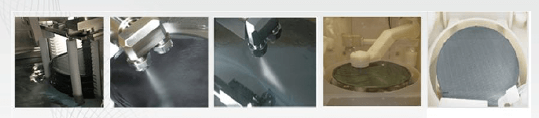
Mauer explained that SSEC has developed two separate systems to address both TSV clean and TSV reveal. TSV clean is a solvent based system that uses a proprietary soak and spray technology. On the other hand, TSV reveal is a spin-on aqueous etch process.
TSV Clean
TSV clean is often overlooked as a critical process step. In reality, it’s essential to reliability. The deep reactive ion etch (DRIE) process used to fabricate TSVs requires rapidly alternating between isotropic plasma etch and fluorocarbon polymer deposition. The passivation pulse results in a polymer residue being left behind on the wafer, which needs to be removed to allow for the defect-free barrier, seed, and fill steps that follow (Figure 1). The process requires both optimized chemistry and the proper tool. SSEC’s contribution to this falls on the equipment side. The company has worked closely with Dynaloy to develop chemistries to support its process.
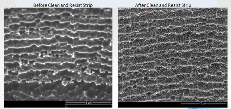
Unlike wet bench or single wafer spray processes, which are the conventional approach to wafer cleaning, SSEC’s soak and spray technology combines equal soak time in the wet buffer tank for each wafer, followed by spray, and then a final clean rinse (Figure 2). Mauer explained that this unique combination improves cost of ownership (CoO) by minimizing spray time and chemistry use, additionally the timed process adds a level of process control because every wafer sees exactly the same process: 30 minute soak, followed by 2 minute spray, and then final rinse. “Every wafer gets its own timer,” said Mauer. “Wafers are continuously loaded into the wet buffer tank. As one goes in, another comes out and goes into the spray chamber. This is unique in the industry.” The significant difference in spray time results in increased throughput, she says. Additionally, the soak and spray combination does a more thorough job of removing the polymer residue than bath only or spray only because the soak time softens the polymer and then it is completely removed with a quick spray step.
TSV Reveal
TSV reveal, the process in which the backside of the wafer is thinned to reveal the copper interconnects, has become an area of focus for process control and improved cost of ownership. Imec’s Eric Beyne identified chemical mechanical planarization (CMP) as one area of possible cost reduction that involves eliminating both CMP and the plasma etch and replacing them with wet etch.
Unfortunately many wet etch processes rely on Tetra Methyl Ammonium Hydroxide (TMAH) as its chemistry formulation – a well known “nasty chemistry” due to its ability to cross the skin barrier if it comes in direct contact with it. Currently, imec is using a TMAH-based, two step reveal process. According to Mauer, SSEC has developed a tool and process that uses Potassium Hydroxide (KOH), which do not share in TMAH’s health concerns. “KOH has a favorable etch rate,” said Mauer. “The challenge is that it leaves potassium silicate residue that has to be removed. But we have an in-situ cleaning process for that, and have ICPMS data (inductively coupled plasma mass spectroscopy) showing its removal.” Mauer added that SSEC is always assessing new chemistries to improve its processes.

Another critical step in TSV reveal is measuring the thickness of the silicon from the point where the copper fill meets the silicon. “There is a non-uniformity in the silicon due to the grind, which is complicated by the varying depths of the vias,” explained Mauer. “Our calculation of silicon thickness minus depth of via provides a desired etch depth profile across the radius of the wafer. Our arm movement is able to compensate for this radial non-uniformity.” Mauer added that its important to see where the vias are revealed to see where to stop the etch. She said SSEC’s tool relies on an optical endpoint with sophisticated algorithms that determines when the vias are revealed. “The optical endpoint is a ‘belt and suspenders’ methodology to ensure that we have complete process control,” notes Mauer. The only other equipment manufacturer who offers end point detection in its etch system is SPTS, but they use dry processes. All others rely on a time-based approach.
Mauer says the advantages of SSEC’s wet etch approach include the elimination of multiple processes tools generally required for dry etch including CMP, plasma etch, metrology, and cleaning. Essentially, one SSEC system configured for TSV reveal replaces four tools required for dry etch process. The company is working directly with SEMATECH as part of SEMATECH’s 3D consortium to prove out CoO of wet etch processes vs. dry etch. The goal is to be able to determine what this buy customers in terms of cost or replace other pieces of equipment.
Be sure to check back on 3D InCites for more ECTC 2013 Interviews. ~ F.v.T


