


We read a lot about the remaining challenges to be addressed before 3D ICs are fully commercialized. Current roadmaps are now targeting 2015 for commercialization of 3D ICs, while 2.5D gets the ball rolling towards the end of 2012, beginning of 2013. Reports from Xilinx indicate they are shipping 2.5D products in thousands, and it’s next-generation 3D product in the hundreds (they’ve added a transceiver to the FPGA slices to make it 3D). At SEMICON West 2012, I met with a number of company’s who’s products address some of these challenges. I call the list ‘incomplete’ because obviously I didn’t get to talk to everybody, just those who contacted me to request a briefing. So if I missed you this year, I apologize. To make up for it, I invite you to use the comment area at the end of this post (it appears if you’re logged in) and add your company’s solution to a particular challenge. So without any further adieu, and in no particular order, here we go.
3D HVM Readiness EV Group is positioning itself for high volume manufacturing, while still working on the temporary bond/debond (TB/DB) conundrum. I caught up with Markus Wimplinger, who told me that the XT Frame handling system that I saw in February when I was visiting the company has been officially released and is ready to go. It can handle double the process modules of the previous system for double the throughput with only a 30-40% footprint increase. It also features inline metrology for pass/fail and rework of bonded wafer pairs. The company is also collaborating with Shin Etsu, making progress in qualifying adhesives for TB/DB. This adds another materials manufacturer to the ZoneBond family in addition to Brewer Science. Wimplinger says this offers customers a choice of materials suppliers which is important for HVM supply chain readiness.
Other big 3D news for EVG is the 11/3 rating the Gemini FB system received from ISMI as a result of its recent equipment maturity assessment. The Gemini FB is reportedly the first 3D related equipment to go through the rating process to achieve this number, and its the best that can be achieved for a tool in a pilot line production, since nothing is in in mass production yet. Gemini IS used in mass production for backside illuminated sensors,which although not a 3D technology, is what helps drives the maturity of the equipment.
Propogating 2.5D Technology and the Transition to 450mm
Ultratech’s recent patent purchase from IBM is helping the company move away from being “just and equipment provider” says Manish Ranjan of Ultratech. The company bought fundamental silicon interposer, TSV, and lead-free packagig related patents to assist customers in propogating the 2.5D and 3D technologies. Customers who purchase Ultratech’s equipment can use the patented process. “This lowers the hurdle rate.” says Ranjan. Additionally, Ultratech has achieved exclusivity status with four companies, and is close to finalizing an agreement for development of a 450mm tool for laser annealing, which while primarily a front-end process, can be leveraged for lithography as both tools are built on the same Unity platform. “Darwinism will help start the program,” says Ranjan, “and will help meet company deadlines for production.
Solving the Via Reveal Issue
While MEMS is where they’re really stealing the show, Dave Thomas of SPTS reports the company is still very active in the 3D space, and has been focusing efforts on via reveal, something Thomas says has been oversimplified and overlooked as a technology. “How do you get high etch rates without a mask? If etch rate and Cost of Ownership (CoO) is everything, how do you control uniformity?” Most people, he said, are favoring ‘soft reveal’, which is a process that is fast and sufficiently uniform, but selective to the TSV liner oxide, so that the copper and silicon don’t “see” each other. The Pegasus Rapier etch tool is outfitted with an endpoint detection system, which allows you to detect the point where the TSV is starting to come through the silicon. The alternative is a flat reveal process that grinds straight in to reveal copper, creating a path for copper diffusion into the silicon which is a bad thing. While Thomas said this isn’t an issue for silicon interposers, its a bad thing for memory and logic parts. While SPTS tools can do either process, the soft reveal is their “sweet spot.”
3D Metrology
Mark Berry, of Metryx, introduced me to the company’s mass metrology technology that is “unique to the industry” and that involves a precision measurement of a wafer’s weight post etch, deposition and via reveal processes. The process is based on the global measurement of mass change on the wafer. If five wafers are put through the same processes, and the mass change is the same, then you know the process is the same. If there is a variation, then the processes were varied. The beauty of this technique, explained Berry, is that it measures areas that can’t be measured by normal metrology processes, such as optical techniques. With it, you can isolate the excursion wafers and find out what’s gone wrong. Its a process monitor for quality control, and tells you overall which wafers are good, and which have something wrong. The company presented a paper focused on this process for TSVs at the SEMATECH Metrology Workshop. It discussed how it can be used to monitor etch processes for creating TSVs, and for monitoring the line of the barrier seed layer.
In the R&D environment, scientists rely on SEM to inspect the wafer for variations in etch, barrier, and seed layer. But SEM is a destructive test, and so in manufacturing you would be testing one wafer out of a hundred, which also affects overall yield. Mass Metrology is a non destructive test that can be done on every wafer during volume manufacturing. It’s meant to be a gatekeeper, identifying the good wafers from the ones that have variations and will need further investigation. After that, other metrology process, such as optical metrology, are employed.

3D Inspection
While officially a metrology process, Robert Newcomb, of Qcept Technologies, introduced me to his company’s unique approach for detecting non visual defects (NVDs) that he says is more of an inspection processes than a metrology process. NVDs do not scatter light, and are therefore not detectable by optical or e-beam inspection tools Qcept Chemetriq process scans the wafer surface to detect changes in materials and charge on the wafer surface by detecting sub-monolayer metallics and organics. As Newcomb explained, every material has its own work function. If you scan the wafer after the backside grind you should see a clean surface. If a defect has a high work function, you can determine what material is causing the contamination. As a result, the process doesn’t just determine that there is an NVD, but it can help determine where in the process flow that a physical defect was first initiated by a precurser NVD. For TSV applications, there’s an added capability that provides a surface height uniformity map. A bump on the surface shows up white, while black indicates a depression. Detection of copper residue combined with surface height information creates unique data for the customer. In an R&D setting, this inspection tool allows researchers to develop and control the process. in manufacturing, it can be used for monitoring process control.
Material Delivery Processes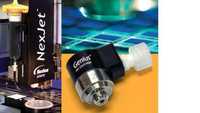 Nordson ASYMTEK is expanding it’s jetting technologies into the 3D space, with its NexJet jetting technology that suits 3D specifications for underfilling fine pitches and tight spaces. The quick-change cartridge features a firing pin inside the jet to control velocity, and therefore size and shape of the dots. It now dispenses =300,000 dps, vs 200,000 dps. According to Akira Morita, Aymtek’s 3D specialist, the company also is looking at how their coating capabilities could be leveraged to accommodate the needs for pre-applied underfill. Spin coating fluid generally results in 95% fluid waste, and Morita says pre-applied laminates prevent that waste and added cost.
Permanant Bonding
I mentioned Ziptronix news of a new license earlier this week, and as promised caught up with Kathy Cook, Business Development Manager, to find out more. In addition to the new license in the handset space, there are others in the works beyond the image space. With regards to further development of the direct bond interconnect (DBI) she said they are moving beyond the company’s internal bonding equipment capabilities, as pitch requirements dip below 2 microns. So collaborative work is underway direct bond interconnect (DBI) technology, she said the company is also doing collaborative work to test the capabilities of commercial equipment as required pitches go below 2um.
“We are going to be testing the capabilities of some of the commercial equipment to see if it can meet sub .5 micron accuracy. we need it to be better than that.” She said, adding that the the DBI technology can meet <.5um accuracy, because unlike thermocompression bonding, the whole process happens inside a bond aligner, and which eliminates 2 out of 3 possibilities for misalignment. "Our technology can make it, and we need to determine which equopment can do it," she said. "There's lots of business potential for those equipment vendors who can do it."
3D Test Equipment
And last but not least, I spoke with Jim Quinn, of Multitest, who updated me on the company’s test handling capabilities for 3D ICs and 3D Packaging. While Multitest doesn’t provide the tester itself, (we need to talk to Advantest or Teradyne for that) they handle the handlers and contactors, as well as load boards. Quinn says because of the company’s long history, particularly in the MEMS market, the company’s Plug and Yield system is suited to partial stack and final test that is needed for testing 3D devices. “We think the yield loss for 3D stacks will be in the assembly process,” explained Quinn. “You have to look at the cost of adding test, compared with the value of not doing it.” OSATS are being mandated to do in-process test, he said, and that test will be a differentiator for 3D. The key is coming up with a cost effective solution. “I think we’re best positioned to do this based on leverage experience, MEMS integration, and the ability to deal with keep-out zones, and high force with high pin counts.”
Complete the List
How is your company positioned to address 3D challenges? We’d like to know. Post your comment here!


