Unlike electrical testing for semiconductors, automating optical test is extremely difficult because of the general finickiness of photonic designs, fragmentation of electronic – photonic design tools, and mechanical precision needed in the test equipment itself.
In order to enable high-volume testing of CPO, more automation is needed to automate existing semiconductor ATE equipment as much as possible. High-volume CPO test needs three forms of automation to coordinate together:
- Electrical ATE for EICs
- Optical instrumentation for PICs
- Mechanical automation for physical handling, precise alignment, and probing
Market Projections for Advanced Packaging and CPO
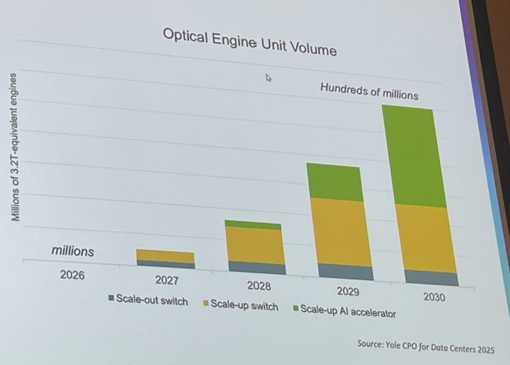
In the next 5 years, both the advanced packaging and optical engine market are projected to grow rapidly due to the need for tighter integration and copper hitting a limit for data speeds. At the SiPh Packaging Summit, Yole projected a huge amount of growth in both markets:
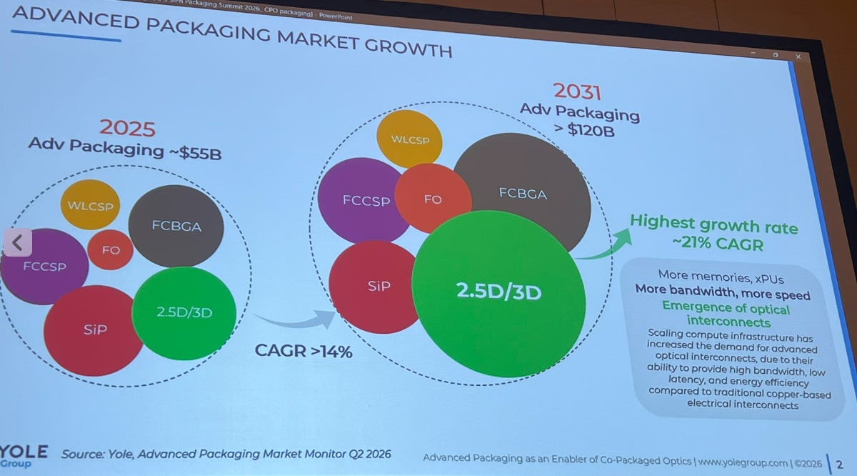
- The advanced packaging market expects growth from $55B in 2025 to >$120B in 2031 with a CAGR of >14%, with much of the growth driven by 2.5D / 3D at ~21% CAGR.
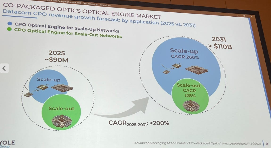
- The CPO market expects growth from ~$90M in 2025 to $110B by 2031, a >200% CAGR mostly dedicated to scale-up.
CPO was initially targeted for scale-out with CPO engines next to switch ASICs to address the faceplate limitations of LPO in large scale data networks. Then, CPO for scale-up / scale-in is following suit to address the BW limitations of copper. Karen Bergman, Professor, Columbia University notes how signals travelling off packaging pay a significant energy penalty and keeping signals on-package has a ridiculous bandwidth ceiling.
However, these market growth rates assume a few things:
- The optical test and measurement ecosystem scales to meet the demand. There is not a well-established, standardized high-volume optical test and measurement ecosystem yet.
- The underlying components have sufficient capacity to meet demand. InP substrate production and CPO fabrication throughput all must scale together to increase manufacturing throughput.
- The reliability of optics doesn’t cause hyperscalers to delay their adoption. CPO engines introduce new reliability risks, where laser failures with a high blast radius could take down a significant portion of a cluster. These risks must not outweigh the power and bandwidth benefits that CPO provides.
Technical Challenges with Optical Test and Measurement
While a lot of equipment and knowhow from semiconductor ATEs can be leveraged, integrating sensitive optical components is challenging. The optical domain tends to be isolated from the electrical domain, requiring equipment manufacturers to develop a broad understanding of how optical works to integrate it properly.

What makes optical test and measurement so challenging? I contend there are four major reasons:
- Precision needed for grating couplers and fibers. Grating couplers are optimized for lasers at a specific angle (typically 8-12 degrees). Single-mode optical fibers have sub-micron positioning tolerances (as low as < 0.5um) to minimize the IL penalty. In contrast, electrical probe needles have a mechanical spring compliance that allows them to scrub pads over a vertical range of 25-75um.
- Warpage on wafers makes precise alignment challenging. A single laser source at the same z-height will experience differing losses depending on the tilt and x-y offset of the wafer underneath.
- Cleanliness. Both dust particles in the air and on the surface block light and cause reflected power and distorted S-parameter measurements that cause otherwise good units to appear as failures. Optical testing environments need to be enclosed in clean environments with automated cleaning mechanisms such as N2 gas nozzles mounted next to optical probe heads.
- Lack of standardization across the optical ecosystem. There is virtually no standardization across several interfaces of the photonic packaging itself, including the optical I/O, optical engines, and optimization instruments.As a result, many CPO players are engaging in their own custom efforts that result in a lot of manual simulation of component libraries. Standardization can cut down on requirements gathering and custom efforts, enabling more market entrants for competitive solutions.
As photonics becomes more tightly integrated, manufacturing economics become increasingly dependent on finding defects earlier—before expensive components are combined.