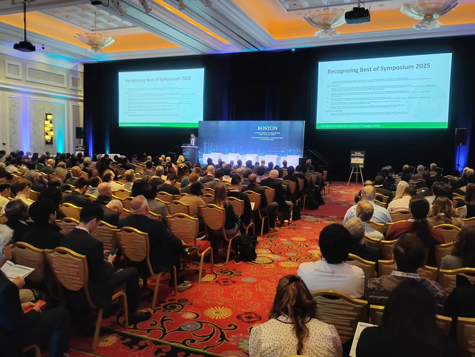
The theme of iMAPS’ 59th International Symposium on Microelectronics, “Intelligent Packaging for the AI Era”, captured the direction of today’s semiconductor packaging industry.
Held September 28 through October 1 at the Encore Boston Harbor Resort, industry leaders explored the technologies enabling next-generation AI and high-performance computing systems, including heterogeneous integration, chiplets, hybrid bonding, advanced interconnects, 2.5D and 3D packaging, photonics, co-packaged optics, and metrology.
Learning Track
Widely regarded as one of the industry’s leading advanced packaging conferences, iMAPS’ annual symposium always brings together researchers, manufacturers, suppliers, and technology innovators from across the semiconductor community.
This year’s symposium featured five technical tracks, more than 100 technical presentations, keynote addresses from industry leaders, professional development courses, expert panel discussions, and a two-day exhibition showcasing the latest innovations in packaging and microelectronics.
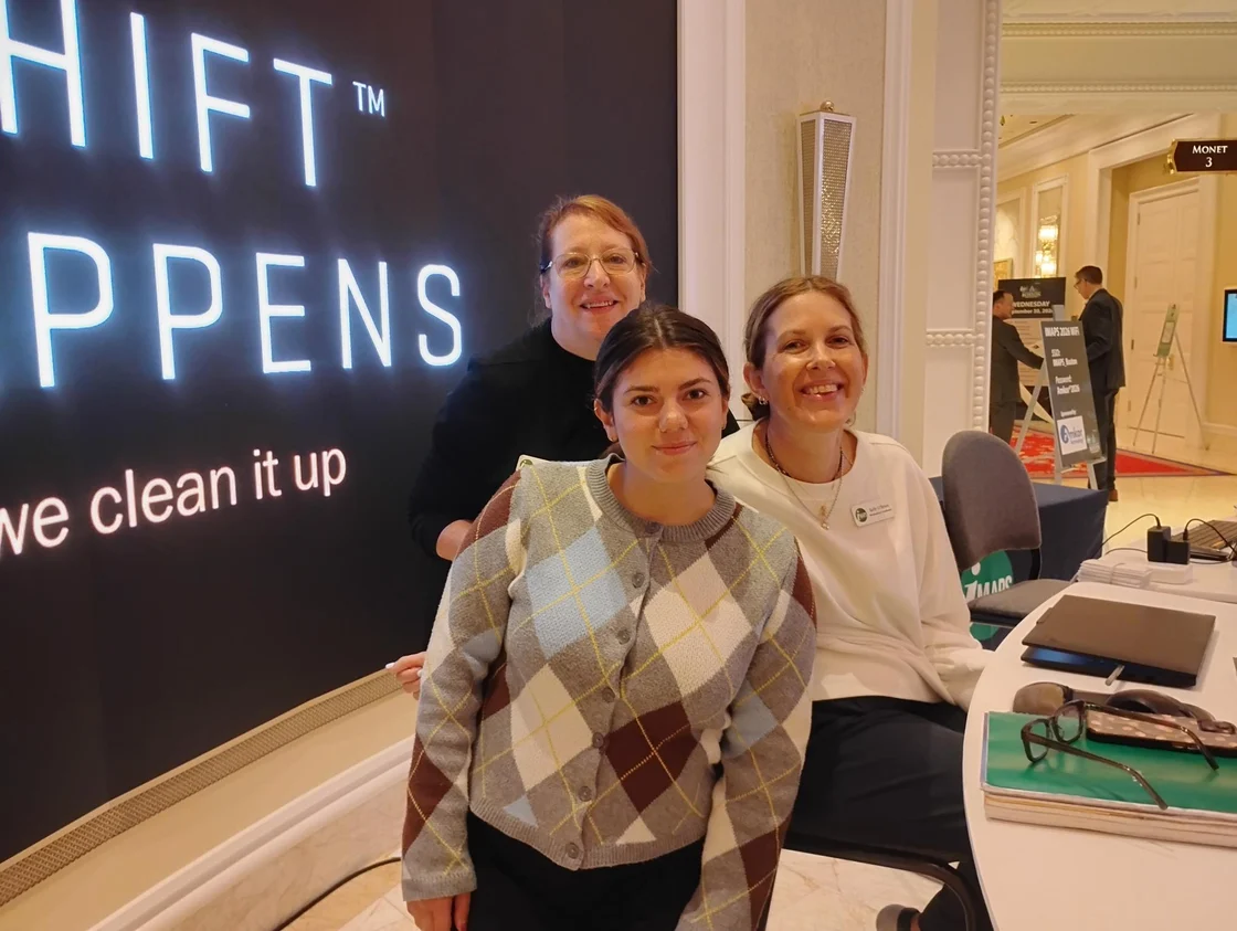
iMAPS staff members Becky Roland, Isabel Volpe, and Kelly O’Brien pause for a break during their very busy schedule!
Measurement Matters
One of the strongest takeaways for VIEW was the growing emphasis on measurement science. A featured panel, Next-Generation Measurement Techniques for Domestic Semiconductor Manufacturing: NIST and Industry Perspectives, underscored the importance of standards, reference methods, and metrology infrastructure as advanced packaging technologies move from development to high-volume production.
As package architectures become more complex, manufacturers need more than defect detection. They need accurate dimensional data that provides insight into process variation, guides corrective actions, and helps ensure repeatable production results. The more advanced the package, the greater the value of precise, actionable measurement data. As advanced packaging enables future breakthroughs, precision metrology is needed to make those innovations manufacturable, scalable, and reliable.

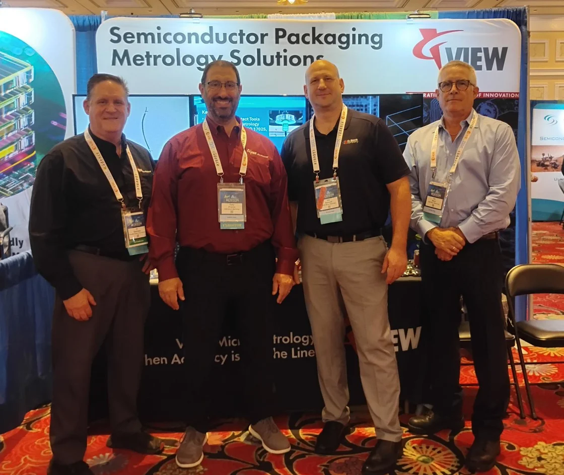
Al Emmans and Tony Frisina of VIEW joined by Jim Bennett and Ian Beck of D. Beck Company, a VIEW Authorized Representative servicing New England
A Standout Week for VIEW
Beyond the technical sessions, iMAPS delivered tremendous engagement for VIEW. Booth activity exceeded expectations and represented the highest level of engagement we have experienced at any trade show to date.
The Symposium provided valuable opportunities to connect with customers, partners, researchers, and industry leaders working at the forefront of advanced packaging innovation. More importantly, it reinforced VIEW’s position in a market increasingly focused on measurement accuracy, process control, and the metrology solutions required to support the next generation of semiconductor manufacturing.