Fan-out wafer-level packaging (FOWLP) has become one of the most important packaging architectures in modern microelectronics. It enables the miniaturization and integration density that powers AI accelerators, high-performance computing systems, and 5G/6G communications without a traditional substrate. Known-good dies are placed on a temporary carrier, encapsulated in epoxy mold compound (EMC), interconnected through redistribution layers, and singulated into finished packages.
FOWLP processes multiple dies simultaneously on a single reconstituted wafer, making it well-suited to the volume demands of AI and communications hardware. In that batch architecture, every design choice carries a direct manufacturing consequence. Mold compound thickness affects die shift during encapsulation. Backside grinding releases residual stresses locked in during molding, altering wafer bow before the first redistribution layer is deposited. Each subsequent RDL introduces additional thermal expansion mismatch between dissimilar materials. Residual stresses accumulate with every process step, ultimately driving wafer warpage.
Out-of-plane deformation of the wafer, or wafer warpage, is determined by design parameters set before fabrication begins: die size, placement density, mold compound thickness, RDL stack-up, and cure cycle. Warpage leads to misregistration of interconnects, violates assembly tolerances, and compromises yield. As domestic packaging capacity scales in USA, warpage prediction and control are key requirements for manufacturable FOWLP at volume.
My doctoral research at Arizona State University addresses this as a unified design-manufacturing problem. I develop thermo-mechanical simulation frameworks that model warpage evolution across the full fan-out build-up sequence, validate them on a live FOWLP prototyping line, and apply machine learning to make predictions fast enough to inform design decisions before fabrication begins.
A critical enabler of this research is ASU’s MacroTechnology Works (MTW), home to the Advanced Electronics and Photonics Core Facility. MTW operates at a process maturity and equipment scale rarely found in a university setting, with a FOWLP prototyping line built on Deca Technologies’ M-Series fan-out platform and Adaptive Patterning process flow. Warpage models are only as credible as the experimental data behind them. Shadow Moiré and Digital Image Correlation (DIC) measurements on wafers processed through MTW’s production-equivalent tools ground simulation predictions in real process conditions. Findings developed at the research level translate directly into process and design guidelines applicable at manufacturing scale.
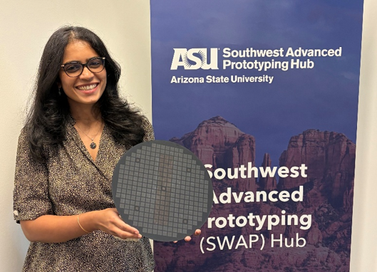
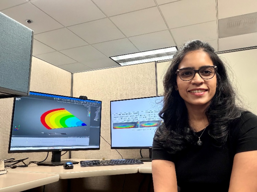
From physical wafer to digital model: a reconstituted FOWLP wafer processed at ASU’s MacroTechnology Works (left) and thermo-mechanical warpage simulation developed in Ansys (right). Bridging these two environments — fabrication and simulation — is the core of my research.
MTW is also the operational hub for SHIELD USA — Substrate-based Heterogeneous Integration Enabling Leadership Demonstration for the USA — a $100M CHIPS/NIST program focused on transforming proven fan-out technology into advanced molded core organic substrates. Leap-ahead targets include ultra-fine pitch chiplet interconnection down to 2 µm and RDL line and space down to 0.5 µm. Achieving those tolerances requires warpage to be predicted and controlled at every stage of the build-up process (SHIELD USA: https://microelectronics.asu.edu/shield-usa/). Within SHIELD USA, my research addresses warpage prediction across the molded core substrate build-up sequence. The thermo-mechanical simulation pipeline and machine learning surrogate I have developed are designed to provide process engineers predictive insight into warpage behaviour before wafer fabrication begins.
A related focus developed a machine learning model guided by the physical properties of EMC to optimize the cure cycle during post-mold curing. The goal is to reduce warpage by designing process conditions that account for material behaviour from the outset. Results were presented at the 2026 IMAPS Device Packaging Conference and IEEE ITherm 2026.
Fan-out packaging also provides a viable avenue for heterogeneous integration of gallium nitride (GaN)devices, the leading semiconductor technology for high-power radar and communications systems. GaN transistors operate at exceptionally high power densities, making thermal distribution across the packaged device a critical reliability consideration. Within the SWAP Hub1 program, funded by DoD/NSTXL, I contributed to electrothermal modeling of GaN-based RF radar systems packaged through ASU’s FOWLP prototyping facility. Simulations characterized thermal behavior across the full package architecture and provided thermal management recommendations for compact RF-GaN integration. Results were presented at GOMACTech2 2026, and an extended study was accepted for oral presentation at the 2026 PSMA 3D PEIM3 conference.

Warpage prediction, cure cycle optimization, and electrothermal modeling for GaN integration are distinct research threads, but they reflect a single underlying principle: advanced packaging is a multi-domain problem. Mechanical, thermal, and electrical behaviour are coupled, and the design and manufacturing of heterogeneous integration systems requires all three to be optimized together rather than addressed in sequence. My research is one contribution to a much larger effort at ASU — a collaborative push toward building the advanced packaging infrastructure that next-generation electronics demand. I am grateful for the opportunity to work alongside researchers, engineers, and industry partners who share that goal, and for the support that enables it.
Pallavi Jithendrriyan is a PhD candidate in Electrical Engineering at Arizona State University, working in Dr. Christopher Bailey’s research group. She is the 2026 IMAPS Scholarship recipient and Co-Chair of the ASU IMAPS Student Chapter.
Footnotes
1 SWAP Hub — Southwest Advanced Prototyping Hub: a DoD/NSTXL-funded program supporting advanced electronics prototyping.
2 GOMACTech — Government Microcircuit Applications and Critical Technology Conference.
3 PSMA 3D PEIM — Power Sources Manufacturers Association, 3D Power Electronics Integration and Manufacturing Conference.