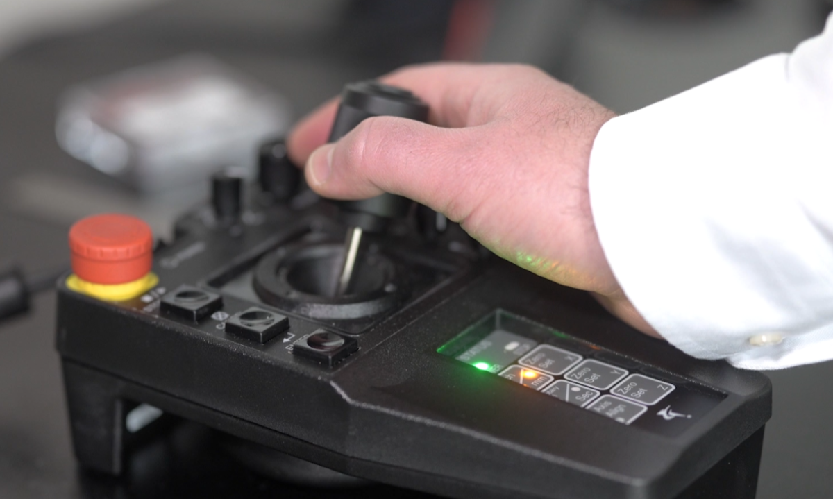
VIEW Micro Metrology is having a productive season in our systems labs in both the United States and Asia, as our applications engineering teams advance a range of internal and customer-driven measurement studies.
The VIEW Micro Metrology Systems Evaluation Lab in Rochester, New York is equipped with a full range of VIEW dimensional metrology tools. This facility supports both internal development efforts and real-world customer applications, enabling both technology validation and process optimization for advanced semiconductor packaging and other manufacturing environments.

High-Throughput BGA Study on 200 mm Wafers
A key study currently underway focuses on measurement throughput for ball grid array (BGA) dies on 200 mm wafers. Each wafer contains approximately 1,300 dies, with each die incorporating 110 solder balls.

The objective of this study is to evaluate both measurement efficiency and data quality in high-volume inspection scenarios, with a focus on:
- A time study comparing Move-and-Measure (MAM) versus Continuous Image Capture (CiC™) strobing recipes on individual solder ball dimensions.
- Defect detection at ball locations across the wafer
- Comparative analysis of ball Z-height measurements using Through-the-Lens (TTL) Laser and Area Multi-Focus (AMF™) 3D imaging
- Repeatability assessment across 25 wafers within the same batch
Results from this study are expected to be published later this Summer.

Gas Distribution Plates → Enabling 100% Inspection at Scale
In addition to wafer-level studies, the lab is currently engaged in a gas distribution plate project involving a semiconductor “showerhead” used in wafer deposition processes. A similar part, though not for use in gas distribution, is undergoing study for a specialized aerospace application.

Vias in gas distribution plates are relatively large (typically >250 µm in diameter) and are well within the capabilities of VIEW measurement systems. However, inspection challenges arise due to requirements for feature uniformity, true position and pitch accuracy, surface topology, and overall positional accuracy.
Defect detection is also often required – particularly on continuously used components – and includes identifying clogged or partially blocked holes, microcracks, pits, residue accumulation, and surface contamination.
Throughput remains a critical consideration for these types of applications from two perspectives:
- Whether the inspection tool can achieve the measurement speed necessary for efficient inline production
- Whether the manufacturer can realistically implement 100% inspection without sacrificing quality
Asia Semiconductor Applications – Expanding BGA and Optical Transceiver Work
Meanwhile, in Thailand, VIEW Authorized Representative V Eye Precision continues to expand application development across both BGA and optical transceiver markets, supporting customers throughout Thailand, Singapore, the Philippines, and Indonesia.


V Eye Precision’s BGA-related work is primarily focused on ball heights and coplanarity – critical parameters for ensuring reliable electrical connectivity and downstream assembly yield.

In parallel, V Eye is advancing metrology applications for optical transceiver manufacturing, highlighting one of the fastest-growing and most demanding areas in semiconductor advanced packaging.

Optical transceiver devices integrate sub-micron photonic structures, fiber interfaces, and precision packaging, all of which demand extremely tight alignment tolerances. Even a ±1 µm shift can significantly impact optical coupling efficiency, underscoring the need for highly-reliable dimensional metrology.
Elevating the Role of Metrology in Advanced Packaging
Across VIEW labs worldwide, these studies are directly aligned with the challenges our customers face every day—driving higher throughput, improving yield, and enabling reliable, scalable inspection in advanced packaging environments.
VIEW’s work consistently demonstrates that metrology is not simply an incremental improvement over AOI – it is a fundamentally different capability. By enabling precise, traceable 3D measurement, VIEW metrology transforms inspection from a reactive quality gate into a proactive engineering tool, empowering customers to detect subtle process shifts, reduce rework, and scale confidently as device complexity continues to increase.

About VIEW Micro Metrology
VIEW Micro Metrology supplies high performance, high accuracy, integrated metrology solutions at or near the production line. Designed for use the semiconductor, electronics, and medical sectors, VIEW solutions utilize advanced non-contact optical metrology systems and versatile software for precise, high-throughput applications. All solutions are turnkey with collaborative design and support for production integration. Additional information can be found on our website.