With the rapidly approaching IMAPS Silicon Valley event, Accelerating Innovation in Advanced Packaging and Heterogeneous Integration with AI on August 11th at Samsung Semiconductor, we thought we’d catch our readers up to speed on last IMAPS event in the Valley, the IMAPS Memory Summit which was hosted by the IMAPS Silicon Valley Chapter, just two months ago in Santa Clara, California.
The discussions and insights shared at the Memory Summit set the stage for the next chapter in the industry’s AI-driven innovation journey. The event presented impressive technical advancements in memory and examined the bottleneck in scaling systems to keep up with the rapidly increasing demand for AI. The Summit was led by General Chair Rozalia Bieca, Field CTO Packaging Technologies at Rapidus Design Solutions and Chair Farhang Yazdani, President and CTO of Broadpak. Industry leaders convened from Samsung, Microsoft, SanDisk, Intel, Mediatek, SK Hynix, AMD, Micron, and many others to tackle the toughest challenge facing the semiconductor and AI industry: the Memory Wall.
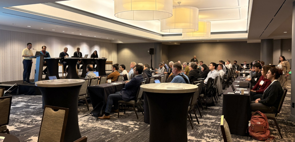
The first Keynote speaker, Rama Shukla, the Vice President of Technology Strategy at Sandisk, presented on his talk, ‘Inferencing-at-scale through Advanced Flash Memory and Packaging Innovations.’ The discussion focused on the issue of memory wall exacerbation with inferencing. He looked at today’s market, relying on the fact that it’s all about accelerator integration and the global shift from training AI models to inference. Shukla stated clearly that “ AI Inferencing scale is the new growth engine.” AI inferencing typically benefits from specialized hardware accelerators that provide high efficiency and low latency.
Models like Grok rely on SRAM-based accelerators, which are highly speed-critical and enable fast computation, but are limited in capacity. In contrast, DRAM, particularly in the form of high-bandwidth memory (HBM), provides much larger capacity and bandwidth, though with higher latency compared to on-chip SRAM. Modern AI systems depend on both memory types, and the efficiency of communication between them is critical to overall performance. This balance between speed and capacity while minimizing latency in data movement was a key theme throughout the conference, highlighting the challenge of optimizing the interaction between these memory layers to reduce bottlenecks associated with the Memory Wall.
A possible solution Shukla sees is High Performance Flash (HPF), which is no longer used solely for long-term storage but is increasingly being deployed for inference workloads and fast data-access layers. As HPF moves closer to the active memory hierarchy, it introduces challenges related to where wear occurs within the flash itself and underscores the need for careful tuning and optimization to achieve high endurance. When managed effectively, HPF can help alleviate pressure on traditional memory layers, making it a potential contributor to overcoming the Memory Wall.
Shahriar Rabbii, president of Majestic Labs AI, spoke on ‘Memory First AI Infrastructure to Overcome the Memory Wall.’ He underscored the obvious gap in the market between computing and memory, primarily on the memory shift, and how design and model deployment are critical at this time in the market. This shift signals a key movement in the market where memory-centric architectures are emerging separately from traditional first compute designs.
However, as we continue to progress down the rabbit hole of AI intelligence, memory, and inference, most of us have our reservations. In his talk, ‘Towards AGI: Reasoning, Introspection and Decision Making’, Microsoft’s Head of Industry Physics and Semiconductors, Preeth Chengappa, began with some bold statistics, comparing Microsoft’s data center power consumption to the power usage of four Hoover dams’ worth of power. This equates to 400 terawatt-hours, putting into perspective the pure scale of infrastructure just around Microsoft’s memory systems alone.
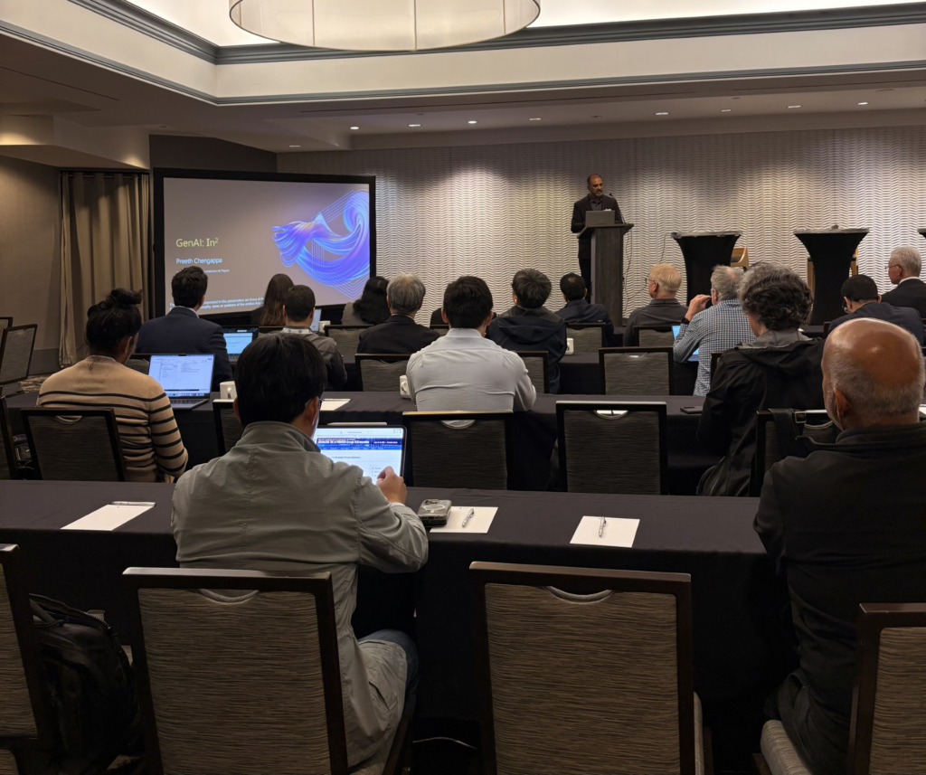
Chengappa is the key integrator of semiconductors and AI at Microsoft, bridging the two and helping the ecosystem navigate the doubling of AI infrastructure from 2025 to 2026. With the boom, he detailed that economic projected growth was wrong, already far surpassing estimates into 2027. The presentation then shifted to market focus and recent news, discussion of the Grok chip, M5 Apple chip, and AMD Instinct were at the top of his list.
He spoke about the reality of AI, referring to the Anthropic Mythos case that he described as just plain scary. This model can find hidden software vulnerabilities and can work bugs into exploitation automatically. He honed in on the fact that these systems must emphasize security, and stated that standardization would benefit all AI platforms.

Security and, perhaps more unexpectedly, introspection topics concluded his talk. AI systems are now beginning to exhibit a form of “regret,” recognizing when they have acted on incomplete understanding or reached premature conclusions. This emerging behavior points to a new level of introspection, where models can reassess their reasoning and adjust outputs accordingly. While not true self-awareness, it reflects a growing ability for AI systems to evaluate their own processes. Still, this capability must be carefully managed, as contextual pruning and oversight are essential to ensure these systems behave appropriately and reliably.
Overall, there was much to take away from this gathering of Silicon Valley leaders. A key theme echoed throughout the conference – the Memory Wall is not a problem that will be solved overnight. In fact, the primary constraint in scaling modern AI and semiconductor systems is no longer compute power alone, but rather memory bandwidth, latency, and the efficient movement of data. Another critical takeaway was the increasing importance of standardization and security across the ecosystem, ensuring that as systems grow more powerful and integrated, they remain reliable, interoperable, and resilient against emerging risks.
On behalf of IMAPS, we would like to extend our sincere thanks to Rozalia Bieca and Farhang Yazdani for their hard work and dedication to the Silicon Valley Chapter and the IMAPS community. We would also like to thank Optalysys for their generous sponsorship of the event and for showcasing their innovative hardware demonstration for computing in transit.
Building on that momentum, the chapter is preparing for another outstanding event next month, bringing together industry experts, researchers, and professionals for valuable technical discussions and networking opportunities. As a continuation of the high-quality programs and industry engagement our chapter is known for, the upcoming IMAPS event reinforces our commitment to delivering meaningful forums that connect the community and advance technology development. Join us next month for the next IMAPS Silicon Valley Event on August 11th at Samsung Semiconductor. The event will bring together an exceptional lineup of speakers from across the semiconductor ecosystem to discuss the technologies enabling the next generation of AI systems.
Representing organizations including AMD, Amkor Technology, Inc., Applied Materials, EV Group, KLA, NAMICS Corporation, University of California, Berkeley, Vinci4D.ai, and more, these experts will share technical insights spanning advanced packaging, heterogeneous integration, manufacturing, simulation, materials, and system innovation.
Visit the event page “Accelerating Innovation in Advanced Packaging and Heterogeneous Integration with AI” for details: https://lnkd.in/gMu3AU8n