VIEW Engineering: The Origins of Automated Optical Metrology
In the 1970s, rapid advances in manufacturing created a growing need for automated optical measurement. CNC machining dramatically increased production speeds, while Statistical Process Control (SPC) required accurate, repeatable measurement data to maintain quality. At the same time, shrinking component sizes and tighter tolerances pushed traditional contact measurement methods beyond their limits, particularly in semiconductor manufacturing.
Responding to Manufacturing’s Emerging Challenges
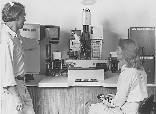
In 1976, physicist and inventor Dr. Richard Alan Hubach discovered that inspecting certain aerospace components cost more than producing them. Recognizing the need for a fully automated, three-dimensional optical measurement solution, he partnered with engineers Veeder South and Jack Sacks to found VIEW Engineering in Canoga Park, California.
Just one year later, VIEW Engineering introduced the RB-1, the world’s first automated three-axis, machine vision-based dimensional measurement system.

VIEW Engineering’s logo, circa 1976
The Birth of Vision-Based Metrology and a New Industry
The RB-1 became the precursor to modern video CMMs. By combining automated image processing, autofocus-driven 3D measurement, and direct SPC data export, it integrated optical inspection, dimensional metrology, and three-dimensional measurement into a single platform. Unlike traditional optical comparators and measuring microscopes, the RB-1 could analyze hundreds of measurement points within a single field of view, dramatically increasing throughput while delivering faster, more accurate, and more repeatable measurements for precision manufacturing applications.e RB-1 became the precursor to modern video CMMs. By combining automated image processing, autofocus-driven 3D measurement, and direct SPC data export, it integrated optical inspection, dimensional metrology, and three-dimensional measurement into a single platform. Unlike traditional optical comparators and measuring microscopes, the RB-1 could analyze hundreds of measurement points within a single field of view, dramatically increasing throughput while delivering faster, more accurate, and more repeatable measurements for precision manufacturing applications.
Building on this success, VIEW Engineering introduced the PR-1 in 1978, the industry’s first pattern recognition system for automated wire bonders and wafer probers, further advancing semiconductor manufacturing automation.
Together, these innovations helped create the modern video metrology market and laid the foundation for decades of advances in machine vision, image processing, and optical metrology that continue to support advanced manufacturing today.
Expansion and Innovation Throughout the 1980s
Disruptive technologies often gain market momentum rapidly when they address a critical industry need. VIEW Engineering’s innovations were no exception. As the semiconductor industry expanded throughout Asia and North America, manufacturers and Outsourced Semiconductor Assembly and Test companies (OSATS) increasingly recognized the value of automated optical metrology. VIEW served these growing markets through a network of authorized sales and service representatives across the United States and Asia, helping establish the company as a global leader in vision-based measurement technology.
In 1981, VIEW Engineering relocated to a larger facility in Simi Valley, California, to support its continued growth and product development initiatives. That same year, the company introduced the VIEW 1200, a second-generation vision measurement platform offering expanded measurement capacity, improved performance, and enhanced automation capabilities.
Strategic Growth and Industry Recognition
The commercial success and technological promise of VIEW’s automated optical metrology soon attracted the attention of major manufacturing organizations. In 1984, automotive giant General Motors made a strategic investment in VIEW Engineering, providing additional resources to accelerate product development and expand the company’s product portfolio.
Shortly thereafter, VIEW introduced new production floor systems that significantly improved edge detection performance and measurement reliability, followed up by one of the industry’s most innovative illumination technologies: the Programmable Ring Light (PRL).
A Breakthrough in Illumination Technology
Invented by VIEW engineer Ralph Weisner in 1985 and protected by patent, the Programmable Ring Light represented a significant advancement in optical metrology. The system utilized movable paraboloidal and toroidal mirrors to create highly controllable illumination angles, providing unprecedented flexibility in highlighting critical part features.
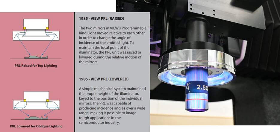
This innovative approach enabled operators to reveal subtle surface characteristics and edge details that were often difficult or impossible to detect using conventional ring-lighting systems. The design was particularly beneficial in semiconductor packaging applications for viewing the tops of reflective metals in wire bonding and ball grid arrays. The result was a substantial improvement in measurement accuracy and reliability, particularly for complex geometries and challenging inspection applications.
Competitors Emerge
As automated optical metrology gained traction during the late 1970s and early 1980s, other innovators recognized the growing demand for highly specialized measurement technologies.
In 1979, Thomas Pelton, an experienced field metrology engineer, founded Micro-Metric, Inc. in San Jose, California. The company focused on developing ultra-precision optical metrology systems for the semiconductor, data storage, flat-panel display, and micro-manufacturing industries. Over time, Micro-Metric earned a reputation for building some of the world’s most accurate optical measurement systems for silicon wafers, magnetic recording heads, sliders, and advanced electronic assemblies.
At the same time, another company was establishing its presence on the East Coast. Under the leadership of Tarry Polidor, Optical Gaging Products (OGP), already known for innovation in dimensional measurement technologies, entered the video metrology market with the introduction of the Vidicom Qualifier 863 at the 1980 International Manufacturing Technology Show (IMTS) in Chicago.
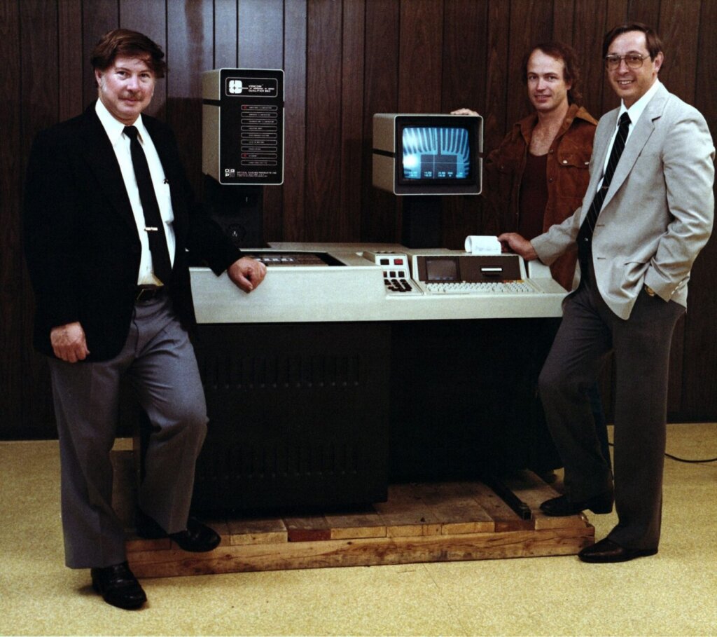
Tarry Polidor, CEO in 1980 (right) poses with the very first Vidicom Qualifier 863 produced by OGP.
Competition among VIEW Engineering, OGP, and other innovators fueled an extraordinary pace of technological advancement throughout the 1980s and 1990s. OGP continued to expand its offerings with the introduction of the Intelligent Qualifier 2000 in 1986 and ultimately the SmartScope® multisensor platform in 1991, helping shape the future of multisensor dimensional metrology.
Together, these companies transformed automated optical measurement from a niche technology into a critical manufacturing discipline serving industries around the world.
Advancing Precision Through the 1990s
VIEW Engineering continued its rapid pace of innovation throughout the 1990s with the introduction of several significant products. As semiconductor devices, data storage components, and electronic assemblies became increasingly complex, VIEW Engineering products helped establish optical metrology as a viable solution for the industry’s most challenging measurement applications.
1999: Pinnacle Systems Introduced
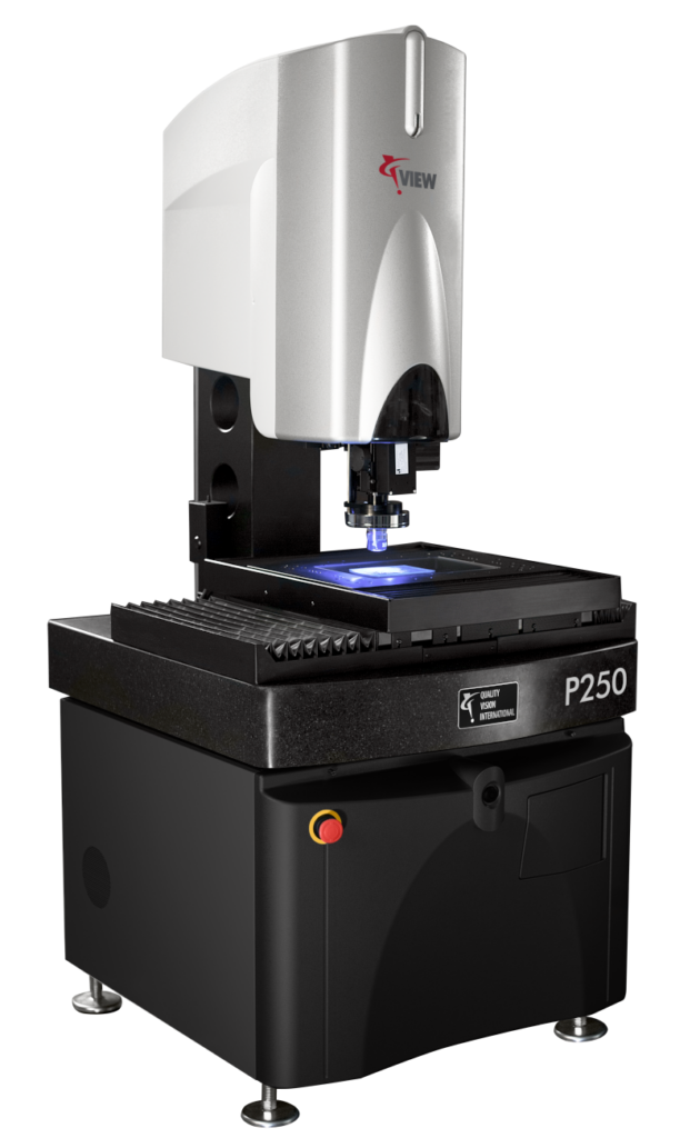
A major milestone followed in 1999 with the introduction of the Pinnacle 250, a versatile and highly capable metrology platform that consolidated decades of VIEW application expertise into a single system architecture.
Designed to measure small, densely packed, and tightly toleranced components, the Pinnacle 250 quickly became a preferred solution for manufacturers across numerous industries. Applications included:
- Chip Scale Packages (CSPs)
- Semiconductor and microelectronic assemblies
- Leadframes
- Ball Grid Arrays (BGAs)
- Hard disk drive suspensions
- Inkjet printer heads
- Precision stampings
Powering the platform was VIEW Measurement Software (VMS), an advanced programming environment that introduced sophisticated automation capabilities, including variables, conditional logic, loops, branching structures, and customizable measurement routines. These features enabled manufacturers to automate complex inspection processes while improving throughput, repeatability, and measurement consistency.

The Pinnacle 250 proved so successful that it remains a key solution in VIEW’s product portfolio today.
Industry Consolidation and the Next Chapter
In 2000, Quality Vision International (QVI), parent company of OGP, acquired VIEW Engineering and expanded its presence in high-precision metrology and semiconductor measurement. Together, OGP and VIEW created one of the industry’s most comprehensive optical metrology portfolios, serving applications from general manufacturing to advanced microelectronics.
VIEW continued to innovate under QVI, introducing the Summit 450 and Summit 600 in 2001. These large-capacity video measurement systems combines high-speed precision stages with fixed-magnification optics to deliver exceptional throughput, accuracy, and repeatability. The Summit platform is a cornerstone of VIEW’s portfolio today, supporting demanding applications such as wafer alignment, panel-level packaging, photomask measurement, and large substrate inspection.
The Formation of VIEW Micro Metrology
QVI strengthened its advanced metrology portfolio in 2006 through the acquisition of Micro-Metric, Inc., a leader in nanometer-scale optical measurement systems for semiconductor and micro-manufacturing applications. The acquisition expanded QVI’s capabilities in critical-dimension and nanoscale metrology while providing Micro-Metric with global sales and support resources.
In 2007, QVI merged VIEW Engineering and Micro-Metric to form VIEW Micro Metrology, combining expertise in semiconductor metrology, machine vision, and high-precision optical measurement. The merger created a stronger platform for innovation and accelerated the development of advanced metrology solutions for customers worldwide.
Asian Markets
As semiconductor manufacturing rapidly expanded across Southeast Asia and China in the late 2000s, QVI increased its investment in the region. In 2009, the company launched its Asia Authorized Channel Partner Program and opened a VIEW Micro Metrology office in Singapore to provide local sales, applications, and service support.
At the same time, VIEW Micro Metrology relocated its U.S. operations from California to QVI’s Western Regional facility in Tempe, Arizona.
Focus on Specialized Semiconductor Markets
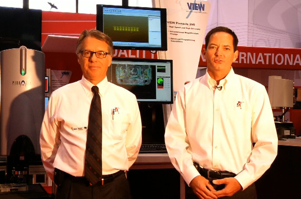
Mark Glowacki and Tim Sladden, former QVI executives who oversaw QVI’s acquisition and merging of VIEW Engineering, Inc. and Micro-Metric Inc.
Under the leadership of QVI executives Mark Glowacky and Tim Sladden in North America, and Raymond Go throughout Asia, VIEW Micro Metrology developed deep expertise in several highly specialized market segments, including:
- Outsourced Semiconductor Assembly and Test (OSAT) providers
- Hard disk drive manufacturing
- Semiconductor tooling and equipment manufacturers
- Probe card manufacturers
- Gas distribution and process equipment suppliers, including showerhead manufacturers

Raymond Go, Managing Director of VIEW Asia based in Singapore, and currently President of VIEW Micro Metrology globally
The Singapore operation successfully established relationships with many of the world’s largest semiconductor manufacturers and assembly providers, while the U.S. division continued supporting customers across diverse industries ranging from aerospace and electronics to medical device manufacturing and precision machining.
Together, these efforts reinforced VIEW Micro Metrology’s position as a global supplier of precision optical metrology solutions for advanced manufacturing environments.
The CHIPS and Science Act Era
During the 2010s, concerns grew as semiconductor manufacturing became increasingly concentrated in Asia, reducing the U.S. share of global production and exposing supply chains to geopolitical and economic risks. These vulnerabilities became especially evident during the COVID-19 pandemic, when chip shortages disrupted industries worldwide.
In response, the United States passed the CHIPS and Science Act of 2022, providing major investments and incentives to strengthen domestic semiconductor manufacturing, research, workforce development, and supply chain resilience.
Establishing the VIEW Micro Metrology Center of Excellence
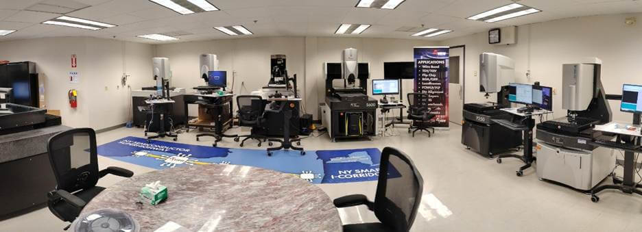
As semiconductor investment accelerated across the United States, QVI realigned its VIEW Micro Metrology operations to support the industry’s resurgence. The company relocated its Tempe office to QVI’s corporate headquarters in Rochester, New York, and in late 2024 established the VIEW Micro Metrology Center of Excellence (COE).
Located within New York’s rapidly expanding semiconductor ecosystem, the facility sits in the heart of the NY SMART I-Corridor Tech Hub, often referred to as New York’s “Semiconductor Superhighway.” The region has emerged as one of the nation’s most significant centers for semiconductor research, manufacturing, workforce development, and technology innovation.
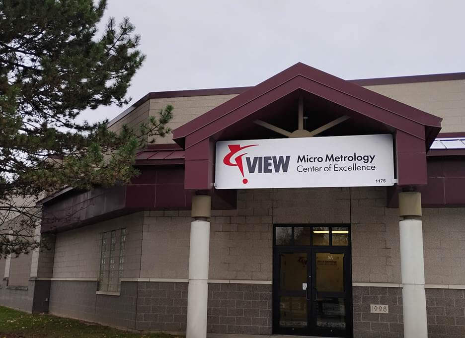
The Center of Excellence serves as a focal point for customer engagement, applications development, and technical collaboration. The facility features:
- A climate-controlled metrology laboratory equipped with VIEW Micro Metrology systems
- Dedicated application development and feasibility study resources
- Advanced software training capabilities
- Customer demonstration and evaluation facilities
- Meeting and collaboration space for semiconductor manufacturers, industry partners, and research organizations
Today, the Rochester Center of Excellence reflects the company’s continued commitment to innovation and customer support while positioning VIEW Micro Metrology at the center of the next generation of semiconductor manufacturing growth in North America.
The Next Chapter
As VIEW celebrates its 50th anniversary, the company reflects on a legacy of innovation that helped shape the field of automated optical metrology. Founded in 1976 by Dr. Richard Alan Hubach, VIEW Engineering pioneered the world’s first machine vision-based dimensional measurement system, establishing the foundation for modern video metrology.
Today, the semiconductor industry stands at the threshold of another transformative era. Advanced packaging technologies, including 2.5D and 3D integration, chiplets, hybrid bonding, high-bandwidth memory (HBM), glass substrates, and heterogeneous integration, are driving unprecedented demands for precision measurement and process control. As critical dimensions shrink and package complexity increases, metrology is becoming more essential than ever to ensure yield, reliability, and performance.
From its Center of Excellence in Rochester, New York, VIEW Micro Metrology continues to develop the optical metrology solutions needed to address these emerging challenges. As it enters its sixth decade, the company remains committed to advancing the science of measurement and supporting the next generation of semiconductor and advanced packaging innovations that will power the technologies of tomorrow.