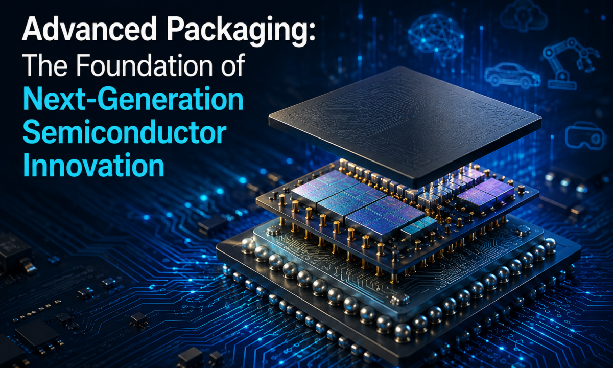
For decades, semiconductor scaling was closely tied to putting more transistors onto progressively smaller areas of silicon. That relationship is becoming less direct as modern systems combine compute dies, high-bandwidth memory, I/O, accelerators, and specialized functions within increasingly dense architectures. Performance now depends not only on what happens inside each die, but also on how efficiently multiple dies can operate together.
Advanced packaging sits at that intersection. Interconnect pitch, memory placement, package dimensions, power delivery, thermal paths and manufacturing yield increasingly influence system architecture. Developments in heterogeneous integration, hybrid bonding, advanced substrates and packaging process equipment point toward a broader change in semiconductor engineering, where the package itself becomes part of the scaling strategy.
AI accelerators and high-performance computing systems make those requirements particularly visible because they place intense demands on bandwidth, data movement and compute density. The underlying shift, however, reaches beyond either application. Next-generation semiconductor devices increasingly depend on how effectively different pieces of silicon can be integrated, connected, powered, cooled, tested and manufactured as one system.
From Monolithic Scaling to Heterogeneous Integration
Large monolithic dies face increasing physical and economic constraints as functionality and die dimensions expand. Reticle limits, defect exposure, process-node requirements and development economics all influence whether functions should remain together or move into separate dies.
Chiplets
Separate compute, I/O and other functions into independently manufactured dies, allowing individual components to use process technologies suited to their requirements.
2.5D Integration
Place multiple dies beside one another through an interposer or embedded bridge, creating dense lateral communication paths without requiring every function to occupy one monolithic die.
3D Integration
Stack dies vertically to shorten selected interconnect paths while introducing tighter requirements around bonding, thermal management, and mechanical reliability.
Package-scale integration is already reaching dimensions that change how system architecture can be approached.
Intel Foundry’s EMIB-T work at ECTC 2026:
- First-layer interconnect bump pitch reduced to 25 µm
- Package form factors reaching 120 × 120 mm
- More than 9× reticles of compute and memory silicon content integrated in one package
- More than 12 Gb/s HBM4e performance
- 64 Gb/s UCIe interface performance
Embedded silicon bridges provide dense lateral 2.5D connectivity, while TSV-enabled vertical scaling supports package-level power delivery. Such architectures allow multiple optimized chiplets to function as a larger computing system without requiring one physically monolithic die.
Interconnect Density Is Becoming a Core Scaling Constraint
Higher die counts solve one architectural problem while creating another: more silicon components must exchange substantially more data through physical interfaces.
- Pitch: Smaller connection dimensions increase the number of interfaces available within a fixed area.
- Bandwidth: Greater connection density creates more capacity for die-to-die communication.
- Alignment: Finer interfaces leave less tolerance for positional variation during assembly.
- Yield: Surface defects, contamination, and bonding imperfections become more consequential as dimensions decrease.
Hybrid bonding is gaining importance precisely because conventional interconnect structures become harder to scale indefinitely.
Imec’s NanoIC pilot line released fine-pitch RDL and die-to-wafer hybrid-bonding process design kits in March 2026. The RDL process supports line widths and spaces down to 1.3 µm, while microbump pitches can reach 20 µm. Imec also reports improvements of up to 40% in communication speed and 15% lower energy per bit on a UCIe-Advanced die-to-die interface for the demonstrated approach.
The engineering significance extends beyond smaller dimensions:
- Surface preparation must remain tightly controlled.
- Bond interfaces must maintain mechanical and electrical integrity.
- Alignment accuracy becomes increasingly important.
- Process variation has a greater impact on yield.
Higher interconnect density therefore requires simultaneous progress in architecture, materials and manufacturing control.
Packaging Is Reworking the Compute-Memory Interface
Memory moves closer to compute
HBM changes the physical relationship between processing and memory. Shorter, denser connections support substantially greater data movement, while package routing, power delivery and validation requirements rise alongside bandwidth.
Validation moves deeper into the package
High-speed interfaces, stacked memory and heterogeneous dies create more variables to evaluate across the completed package.
Signal integrity, thermal behavior and reliability increasingly become part of the same validation problem.
Test follows the integration curve
Rising integration density is also expanding the need for more advanced semiconductor test capabilities, with South Korea’s semiconductor test equipment market projected to grow at a 6.33% CAGR from 2026 to 2032, supported by HBM, advanced memory, AI chips and increasingly complex package validation.
Packaging and test consequently move closer to the architecture itself. Higher integration density means verifying interfaces and package-level performance becomes part of getting the system into production.
Higher Integration Density Raises Power and Thermal Demands
Higher package density brings more compute and memory into the same physical space, increasing the amount of power that must be delivered and heat that must be removed.
Thermal and mechanical effects therefore become closely tied to how densely dies, interconnects, and substrates are integrated.
Power concentration:
- More active silicon occupies a smaller package footprint.
- Localized power density can increase thermal loads.
- Power-delivery structures must operate alongside dense signal routing.
Thermal behavior:
- Silicon, interposers, substrates, and bonding materials respond differently to temperature changes.
- Larger packages become more sensitive to warpage and thermal-expansion mismatch.
- Stacked structures can create more difficult heat-removal paths.
Reliability consequence:
Repeated thermal cycling and mechanical stress can degrade package interfaces over time. Bond integrity, material interaction, and structural stability therefore need consideration during package development rather than after assembly.
Thermal design consequently becomes part of the architecture itself. Greater integration density is useful only when power and heat remain within manageable operating and reliability limits.

Advanced Packaging Is Also Becoming a Manufacturing Challenge
RDL formation
Fine routing depends on tighter control of line dimensions, dielectric behavior, and plating uniformity.
TSV processing
Vertical interconnects require consistent geometry, sidewall quality, filling and defect control.
Bond preparation
Surface condition and alignment directly affect interface quality and connection yield.
Inspection
Hidden defects become more difficult to identify as packages contain stacked or embedded structures.
Metrology
Thickness, overlay, warpage, and dimensional variation increasingly require close process monitoring.
3D InCites’ April 2026 coverage of wafer-level and panel-level packaging points to wet processing, electrochemical plating, PECVD and panel-level packaging as important process technologies for increasing packaging precision, performance and scalability.
India’s packaging infrastructure is already reflected in its equipment mix, with assembly and packaging equipment accounting for 38% of the semiconductor manufacturing equipment market in 2026.
Packaging-related projects require equipment spanning:
- Dicing and singulation
- Die bonding
- Wire and flip-chip bonding
- Molding and encapsulation
- Inspection and process control
- Wafer probing and final test
Process repeatability increasingly determines whether complex package architectures can achieve commercial yield.
Scaling the Package Requires New Substrate Architectures
Larger package footprints are increasing the demands placed on the substrate itself. Routing density, dimensional stability, and warpage control now have to be considered alongside electrical performance.
- Panel formats: Larger processing areas can improve throughput and manufacturing economics, while greater surface area makes uniformity, warpage and handling harder to control.
- Large package dimensions: More compute dies and memory devices require greater routing capacity, placing additional pressure on power distribution, signal integrity and mechanical stability.
- Glass-core substrates: SEMI and Global Net Corp.’s 2026 research identifies glass-core substrates as a potential $13 billion opportunity by 2040, with flatness, rigidity, thermal stability and CTE alignment among the properties supporting their development for larger advanced packages.
Substrate engineering is consequently becoming part of the scaling equation. Material properties can influence package dimensions, routing density and mechanical behavior alongside the choices made for dies and interconnects.
Where Electrical Interconnect Starts to Push Packaging Toward Photonics
Electrical links remain central to package communication, but rising bandwidth requirements are placing greater pressure on conventional interconnect architectures.
Co-packaged optics is emerging in response to that pressure by moving optical connectivity closer to the computing package.
- Shorter electrical paths: Placing optical interfaces closer to computing hardware can reduce the distance that high-speed electrical signals need to travel before conversion.
- Higher data movement: Optical connectivity provides another route for handling increasing volumes of data across high-performance computing systems.
- Alignment becomes critical: Optical coupling depends on precise positioning between components, making assembly accuracy more demanding than in conventional electrical connections.
- Thermal and mechanical effects remain: Bonding conditions, temperature changes, and mechanical movement can alter optical alignment and affect long-term package performance.
- Manufacturing repeatability determines scalability: 3D InCites’ July 2026 coverage of silicon photonics packaging identifies active and passive alignment, bonding precision, thermal behavior and manufacturing repeatability as important challenges in moving photonic packages toward volume production.
Optical integration therefore changes the packaging problem rather than removing it. Greater bandwidth can be supported through photonic connectivity, but package assembly must achieve the alignment, stability and repeatability required to make that architecture practical at scale.
The Next Constraint Is the Integration Chain
Advanced packaging now spans too many interdependent processes for one technology to determine success on its own.
- Yield: More dies and interfaces introduce additional opportunities for manufacturing loss.
- Reliability: Bonding interfaces, thermal cycling and interactions among multiple materials must remain stable through the product lifecycle.
- Test coverage: Validation has to extend across individual dies, interfaces and the completed heterogeneous package.
- Interoperability: Chiplet-based architectures require compatible die-to-die interfaces and coordinated design methodologies.
- Manufacturing capacity: Specialized packaging lines, equipment, materials and engineering expertise must expand alongside architectural complexity.
Capacity expansion is already becoming a strategic consideration.
Amkor and NVIDIA announced a multi-year partnership in July 2026 that includes a $1.5 billion advanced packaging and development agreement to support expansion of Amkor’s U.S. advanced packaging capacity and development of technologies for next-generation AI and accelerated computing platforms. The companies also plan to align roadmaps around high-density interconnects and heterogeneous integration.
Packaging infrastructure is therefore becoming part of semiconductor competitiveness. Architectural progress can advance only as quickly as production ecosystems can reproduce new package structures at acceptable yield, reliability, and cost.
Advanced Packaging Is Becoming a Semiconductor Scaling Layer
Packaging once sat largely downstream of semiconductor design. Modern heterogeneous systems are changing that relationship as package-level decisions increasingly influence how compute, memory, interconnect, and power functions are brought together.
- Architecture now depends on packaging: Compute partitioning affects package design, while memory bandwidth influences routing density and interconnect requirements.
- Performance now depends on physical integration: Interconnect pitch affects bonding and yield, while higher power concentration increases the importance of thermal design.
- Package dimensions now influence manufacturing: Larger footprints affect substrate selection, mechanical stability, process control, and the ability to reproduce complex structures at scale.
Developments across 2026 reinforce the same direction. Multi-die integration is expanding package scale. Hybrid bonding is pushing interface density. HBM is increasing requirements around memory integration and testing. Advanced substrates are addressing package-level limitations, while optical connectivity is opening another path for high-bandwidth communication.
What this Means for Semiconductor Scaling
Future progress will depend not only on smaller transistors, but also on how effectively different pieces of silicon can be integrated, connected, powered, cooled, tested and manufactured as one system.
Advanced packaging is becoming the layer where those requirements converge. Its role is therefore shifting from supporting semiconductor innovation to helping define what the next generation of semiconductor systems can achieve.
Author Bio:
Pooja Dhoundiyal is a Research Manager at Vyansa Intelligence with an engineering background and more than nine years of experience in market research. She leads research initiatives across advanced technology sectors, with a focus on semiconductor packaging, microelectronics and emerging semiconductor technologies. Her work combines technical research with industry analysis to assess technology developments, market dynamics and evolving requirements across the semiconductor ecosystem.