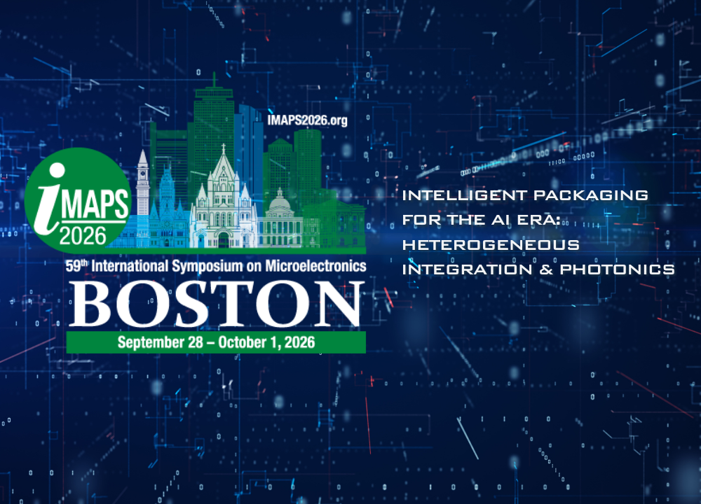
The International Microelectronics Assembly and Packaging Society (IMAPS) will host the 59th International Symposium on Microelectronics (IMAPS Symposium 2026) from September 28 to October 1, 2026, at the Encore Boston Harbor in Everett, Massachusetts.
Centered on the theme, Intelligent Packaging for the AI Era: Heterogeneous Integration and Photonics, this year’s Symposium reflects the growing role of advanced packaging as a system-level enabler. AI and high-performance computing are driving greater demands for compute density, memory and I/O bandwidth, power delivery, thermal management, and reliability. Meeting these demands requires the coordinated integration of compute, memory, interconnect, power, and photonic functions—a challenge reflected throughout the program in sessions spanning bonding, chiplets, advanced substrates, optical integration, metrology, modeling, and AI-enabled design and inspection. In this context, “intelligent packaging” refers both to the architectures that enable advanced computing and to the increasingly capable tools used to bring them from concept through manufacturing and qualification.
At its core, the IMAPS Symposium is about community. It is a place where specialists can go deep while also connecting across disciplines, companies, and generations. Students, early-career professionals, and first-time attendees are encouraged to introduce themselves, ask questions, and take full advantage of the access this community offers. Many of the most valuable ideas and lasting professional relationships begin in the conversations between sessions.
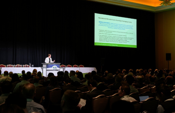
IMAPS 2026 begins on Monday, September 28 with 16 Professional Development Courses (PDCs) designed to provide attendees with practical, expert-led training on key industry topics. This year’s PDCs will include topics such as Hybrid Bonding; Co-Packaged Optics/Photonic Chiplets; Substrates & Interposers; 3D Packaging; FOWLP; Modeling/Simulation; Cost Breakdown of Advanced Packaging; Thermal Interface Materials; and more. These 16 two-hour PDCs will be taught by industry subject-matter experts from organizations such as Intel, ASE, Texas Instruments, Unimicron, Fraunhofer IZM, and Kulicke & Soffa, among others. Monday afternoon also features the panel, “Next-Generation Measurement Techniques for Domestic Semiconductor Manufacturing: NIST and Industry Perspectives,” highlighting the metrology, reference methods, and standards required to scale emerging technologies. New this year, our student-industry program includes Semiconductor 101, Packaging 101, and a social mixer designed to introduce high school students, undergraduates, and their families to the opportunities within the microelectronics industry.
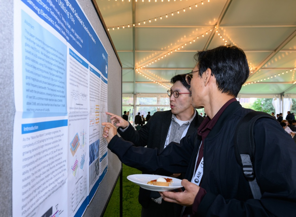
The three-day technical conference runs from September 29 through October 1 and features five technical tracks comprising 22 sessions on a wide range of advanced packaging topics. The program includes more than 135 presentations by subject-matter experts from industry, government, and academia around the globe. This year’s program will also feature four distinguished keynote speakers from Qualcomm, Cerebras Systems, IBM, and Marvell Technology, along with expert panel discussions, special invited sessions, a poster session, and extensive networking opportunities. The panel sessions will examine two timely topics: “Hybrid Bonding for Heterogeneous Integration” and “Packaging Challenges in the AI Era: Substrates and Interposers Shortages.”
In parallel with the conference, attendees can explore a dynamic, sold-out Exhibition Hall on September 29 and 30, featuring companies from across the microelectronics and advanced packaging supply chain. The technical program shows us what is becoming possible; the exhibition provides a close look at the equipment, materials, processes, design tools, and manufacturing capabilities making those advances real.
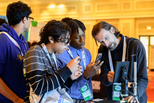
Attendees are encouraged to attend a session outside your usual specialty, engage with a student or first-time attendee, visit the exhibition, reconnect with colleagues, and make new connections. The challenges before our industry are too interconnected for any one discipline or organization to solve alone, and IMAPS and our industry are at their best when we learn from one another.
Event Details:
• Conference: September 28 – October 1, 2026
• Exhibition: September 29 – 30, 2026

• Professional Development Courses: September 28, 2026
• Location: Encore Boston Harbor, 1 Broadway, Everett, MA 02149
Following the IMAPS Boston Symposium, from October 1-2, the IMAPS Si-Photonics Packaging Summit will commence, at the Encore Boston Harbor Hotel. This summit is dedicated to advancing the state of the art in silicon photonics and co-packaged optics. Bringing together leaders from across the silicon photonics ecosystem, including IDM and fabless companies, foundries and OSATs, EDA and equipment/material suppliers, academia, research institutes, and market research organizations, the summit aims to provide a focused forum for sharing insights, discussing challenges, and fostering collaborations in silicon photonics packaging.
Both the 59th International Symposium on Microelectronics (IMAPS Symposium 2026) and the Si-Photonics Packaging Summit offer premier opportunities to learn about emerging technologies, connect with industry experts, and stay at the forefront of microelectronics packaging innovation.
Exhibitor Information: