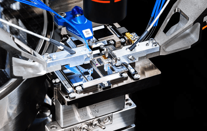
The rapid development of artificial intelligence (AI), high-performance computing (HPC), and hyperscale data centers is creating unprecedented demand for bandwidth between processors, memory, switches, and storage systems. As GPU and accelerator performance continues to increase, moving data between compute resources is becoming an increasingly important part of overall system performance and energy consumption.
Traditional copper-based electrical interconnects remain highly effective for short distances, but their insertion loss, signal integrity requirements, equalization overhead, and power consumption become increasingly challenging as data rates and link distances increase. As a result, optical interconnect technologies are becoming increasingly important for high-bandwidth systems.
Silicon Photonics (SiPh) has emerged as one of the leading approaches for integrating optical communication functions with semiconductor manufacturing and advanced packaging. More importantly for next-generation systems, Silicon Photonics is increasingly being combined with 2.5D/3D packaging, chiplets, advanced substrates, and Co-Packaged Optics (CPO).
Rather than simply replacing electrons with photons, the industry is moving toward a more integrated architecture in which electrical and optical technologies are co-designed at the package and system levels.
I. What Is Silicon Photonics?
Silicon Photonics is a technology platform for implementing optical functions on silicon-based substrates, commonly using silicon-on-insulator (SOI) wafers. A silicon photonic integrated circuit (PIC) can incorporate optical waveguides, modulators, splitters, couplers, filters, and photodetectors together with electronic control circuits.
The basic principle is straightforward: electrical data is converted into an optical signal, transported through an optical waveguide or fiber, and subsequently converted back into an electrical signal at the receiver.
However, describing this process simply as data “traveling at the speed of light with negligible loss” is misleading. The optical carrier propagates at a velocity determined by the refractive index of the waveguide rather than the vacuum speed of light, and practical optical links experience waveguide loss, coupling loss, connector loss, bending loss, and other impairments.
The key advantage of photonics is therefore not that optical signals experience zero loss or consume zero power. Instead, optical interconnects can provide favorable bandwidth-distance characteristics and avoid some of the frequency-dependent attenuation and equalization challenges associated with high-speed electrical links.
This distinction is particularly important in large AI and HPC systems where electrical interconnects may need to operate over increasingly demanding distances.
II. Key Components of a Silicon Photonic System
A silicon photonic system generally combines silicon photonic devices with optical sources, electronic drivers, receivers, and packaging technologies.
1. Light Sources
Silicon has an indirect bandgap and is not an efficient material for conventional laser emission. Consequently, practical Silicon Photonics systems commonly rely on external laser sources or integrate III-V semiconductor materials such as indium phosphide (InP) through heterogeneous or hybrid integration.
The laser architecture has an important impact on system power, thermal management, reliability, and packaging complexity.
For example, an optical engine may use a remotely located continuous-wave laser while performing modulation on a silicon photonic chip. Other architectures seek tighter integration between the laser source and the photonic integrated circuit.
Therefore, the laser should be considered an important part of the overall optical system rather than simply an accessory to the silicon photonic chip.
2. Optical Waveguides
Waveguides perform a role similar to electrical traces, guiding optical signals between different photonic devices.
Silicon’s relatively high refractive index enables strong optical confinement, allowing compact waveguide structures to be fabricated using semiconductor manufacturing processes.
However, waveguides still exhibit propagation loss. Additional losses can occur at bends, couplers, fiber interfaces, and other transitions. These losses must be included in the optical power budget during system design.
3. Optical Modulators
Optical modulators convert electrical information into changes in an optical carrier. Depending on the architecture, modulation can involve the optical signal’s amplitude, phase, or other properties.
Silicon photonic platforms commonly employ mechanisms such as carrier-depletion or carrier-injection modulation, including devices based on Mach-Zehnder interferometers and ring resonators.
Although optical modulation can reduce certain interconnect losses compared with long electrical links, modulators are not inherently zero-power devices. Their energy consumption depends on device architecture, drive voltage, capacitance, modulation format, operating speed, and associated driver electronics.
System-level power must also account for the laser, driver, receiver, clocking, control circuits, and potentially DSP functions.
4. Photodetectors
Photodetectors convert optical signals back into electrical signals.
Silicon itself is not ideal for detecting longer-wavelength telecom-band light around 1310 nm and 1550 nm, so germanium-on-silicon photodetectors are widely used in silicon photonic platforms.
Receiver performance affects sensitivity, bandwidth, optical power requirements, and ultimately the total link budget.
5. Optical Couplers and Fiber Interfaces
Efficient coupling between the photonic die and optical fiber is one of the most important packaging challenges.
Two common approaches include edge coupling and grating coupling. Each has different implications for coupling efficiency, alignment tolerance, wafer-level testing, packaging, and manufacturing cost.
For advanced packaging applications, optical coupling is increasingly becoming a packaging-engineering problem rather than purely a photonics problem.
III. Why Silicon Photonics Is Important for AI and HPC
The growth of AI workloads has changed the balance between compute and communication.
Modern accelerators can perform enormous numbers of operations per second, but distributed computing requires data to move between GPUs, CPUs, memory systems, switches, and other accelerators.
As aggregate bandwidth increases, the interconnect itself can become a significant contributor to system power and latency.
1. Bandwidth-Distance Scaling
Copper remains extremely competitive for short electrical connections. However, as signaling rates increase, channel loss and signal integrity become more difficult to manage.
Electrical links can require sophisticated equalization, retimers, PCB materials, connectors, and power-hungry SerDes circuits.
Optical links offer a different scaling path. Multiple wavelengths can potentially share the same optical infrastructure through wavelength-division multiplexing (WDM), while optical fibers can maintain high bandwidth over distances that would be increasingly difficult for conventional PCB traces.
Consequently, the industry is not moving toward “optics everywhere.” Instead, a more realistic direction is to use electrical signaling where it remains efficient and transition to optical interconnects where bandwidth, distance, or power constraints justify the additional optical complexity.
2. Power Efficiency at the System Level
One of the strongest arguments for optical interconnects is the potential to improve energy efficiency for appropriate link distances and bandwidth requirements.
However, it is inaccurate to state that optical propagation itself consumes virtually no power and therefore makes the entire optical link extremely low power.
A practical optical link includes:
- Laser power
- Modulator driver power
- Modulator losses
- Receiver power
- TIA power
- DSP or SerDes power
- Thermal management
- Optical coupling losses
- Electrical-to-optical and optical-to-electrical conversion overhead
The relevant engineering metric is therefore energy per bit at the system level, rather than the power consumption of the optical waveguide alone.
This is particularly important for AI systems, where thousands of high-speed links can collectively represent a substantial fraction of platform power.
IV. From Silicon Photonics to Co-Packaged Optics
Silicon Photonics becomes particularly interesting when combined with advanced semiconductor packaging.
Historically, high-speed optical transceivers have commonly been implemented as pluggable optical modules located at the front panel of a networking system.
This architecture provides important advantages:
- Easy field replacement
- Mature manufacturing infrastructure
- Independent optical module qualification
- Relatively straightforward system maintenance
- Flexibility in upgrading optical modules
However, the electrical path between a switch ASIC and a front-panel optical module becomes increasingly challenging as signaling rates increase.
The PCB traces and electrical connectors between the ASIC and optical module introduce insertion loss and require increasingly sophisticated signal conditioning.
This creates a fundamental architectural question:
What happens if the optical engine is moved much closer to the switch ASIC?
This is the motivation behind Co-Packaged Optics (CPO).
V. Pluggable Optics vs. Co-Packaged Optics
In a conventional pluggable architecture, the optical transceiver is physically separated from the main switching ASIC.
The electrical signal travels from the ASIC through the package, PCB, connectors, and module interface before being converted into an optical signal.
In a CPO architecture, optical engines are positioned much closer to the switching ASIC, potentially within the same package or package-level assembly.
The objective is not simply miniaturization.
The more important goal is to shorten the high-speed electrical path between the ASIC and optical conversion point.
This can reduce electrical channel loss and potentially reduce the need for aggressive equalization or signal conditioning.
The tradeoff is that CPO introduces substantial packaging challenges.
A pluggable module can be replaced relatively easily. A co-packaged optical engine is much more tightly integrated with the primary silicon and therefore becomes part of the package manufacturing, qualification, reliability, thermal, and test strategy.
This is why CPO is fundamentally an advanced packaging problem as well as an optical interconnect problem.
VI. Why 2.5D Packaging and Chiplets Matter
The development of CPO is closely related to the broader semiconductor industry’s transition toward 2.5D and 3D heterogeneous integration.
A modern high-performance package may contain:

- A large switch or accelerator die
- Multiple chiplets
- High-bandwidth memory (HBM)
- Silicon interposers
- Power delivery structures
- Optical engines
- Photonic integrated circuits
- Electrical SerDes interfaces
A 2.5D silicon interposer can provide high-density electrical connections between multiple dies while also serving as part of the physical infrastructure for heterogeneous integration.
Chiplet architectures further allow different functions to be manufactured using different process technologies. For example, compute logic may use an advanced CMOS node, while I/O, analog, optical, or specialized functions may use other processes.
For photonics, this separation can be particularly valuable because the best manufacturing process for a high-performance digital processor is not necessarily the optimal process for photonic devices, lasers, photodetectors, or optical drivers.
Therefore, heterogeneous integration allows designers to combine different technologies within a common package instead of forcing every function onto a single semiconductor process.
VII. The Role of Hybrid Bonding
As interconnect density continues to increase, traditional solder bumps and microbumps face scaling limitations.
Hybrid bonding provides another potential technology path for advanced heterogeneous integration.
Unlike conventional solder-based interconnection, hybrid bonding can create direct dielectric-to-dielectric bonding together with fine-pitch metal-to-metal connections.
This enables much finer interconnect pitches and shorter electrical paths between dies.
For photonics and CPO, fine-pitch bonding could potentially enable tighter integration between:
- Photonic integrated circuits
- Electronic driver ICs
- Optical engines
- Switch ASICs
- Other chiplets
However, hybrid bonding introduces demanding requirements for wafer and die cleanliness, surface planarity, alignment accuracy, bonding temperature, yield, and defect control.
For packaging engineers, these manufacturing considerations are just as important as the photonic device performance itself.
VIII. Thermal Management Becomes a Critical Packaging Issue
One of the most important differences between conventional optical modules and CPO is thermal integration.
A high-performance switch ASIC can dissipate hundreds of watts, while optical engines and their associated electronics may have their own temperature constraints.
Photonic devices can also be sensitive to temperature because changes in temperature affect the refractive index and therefore the behavior of resonant and interferometric structures.
This creates a difficult packaging problem:
How can high-power electronic devices and temperature-sensitive photonic devices coexist within the same package?
Potential solutions include:
- Advanced heat spreaders
- High-performance thermal interface materials
- Improved package-level heat paths
- Thermal isolation structures
- Active thermal control
- Wavelength or bias compensation
- Careful optical-engine placement
Thermal simulation therefore needs to be performed together with optical and electrical design rather than being treated as a final packaging step.
IX. Optical Alignment and Packaging Tolerances
Optical coupling presents another major challenge.
Electrical connections can often tolerate relatively straightforward mechanical assembly tolerances. Optical coupling, however, can be highly sensitive to positional errors.
The challenge involves multiple dimensions:
- X/Y alignment
- Vertical alignment
- Angular alignment
- Fiber-array placement
- Coupler geometry
- Adhesive shrinkage
- Thermal expansion
- Package warpage
For high-volume manufacturing, active optical alignment can improve coupling performance, but it also increases manufacturing complexity and cycle time.
Passive alignment strategies are therefore attractive when the optical design and packaging process can provide sufficient tolerance.
This creates a fundamental engineering tradeoff between:
optical performance, alignment tolerance, manufacturing throughput, and cost.
X. Wafer-Level Testing and High-Volume Manufacturing
Testing Silicon Photonics is also different from conventional electronic wafer testing.
Electrical devices can often be contacted directly using conventional probe cards. Photonic devices require an optical interface.
Wafer-level photonic testing may involve:
- Fiber arrays
- Grating couplers
- Edge couplers
- Optical probes
- Automated alignment
- Optical power measurement
- Wavelength characterization
- Bit-error-rate testing
- Thermal characterization
The goal is to identify defective photonic dies before expensive packaging operations.
This is particularly important because packaging a defective photonic die can add significant cost.
For high-volume production, the industry therefore needs test architectures that combine high alignment accuracy with high throughput and repeatability.
XI. Manufacturing and Reliability Challenges
Despite its advantages, Silicon Photonics still faces several challenges before it can become a universal interconnect technology.
Laser Integration
Efficient and reliable integration of III-V lasers with silicon photonics remains an important area of development.
Different approaches—including external lasers, hybrid integration, and heterogeneous integration—offer different tradeoffs in performance, cost, reliability, and packaging complexity.
Process Variability
Photonic devices can be sensitive to dimensional variations in waveguides, resonators, and couplers.
Manufacturing tolerances therefore need to be considered during both device design and system calibration.
Thermal Stability
Temperature changes can affect optical characteristics and require compensation or thermal control.
Packaging Yield
As the number of optical and electrical interfaces increases, package yield becomes increasingly important.
A CPO assembly may contain multiple dies, optical connections, electrical connections, thermal interfaces, and other components. The final system yield is therefore affected by the yield of each individual manufacturing step.
XII. Silicon Photonics and the Future of Advanced Packaging
Silicon Photonics should not be viewed simply as a replacement for copper.
Its larger significance lies in the convergence of photonics, semiconductor processing, advanced packaging, and high-performance computing.
The future architecture is likely to contain a mixture of electrical and optical interconnects.
Short-distance communication inside a package may remain electrical because copper and advanced package interconnects can provide excellent performance over short distances.
Optical links become increasingly attractive as bandwidth and distance increase.
This creates a hierarchy of interconnect technologies:
Transistor → Die → Chiplet → Package → Board → Rack → Data Center
At each level, engineers can select the most appropriate electrical or optical technology according to bandwidth, distance, latency, power, cost, and manufacturability.
CPO represents one important step in this evolution by moving optical conversion closer to high-bandwidth compute and networking silicon.
XIII. Conclusion
Silicon Photonics is becoming an increasingly important technology for addressing the bandwidth and energy challenges associated with AI, HPC, and hyperscale data centers.
However, its value should not be described simply as “data traveling at the speed of light” or “zero-power optical transmission.” Real optical systems contain lasers, modulators, drivers, receivers, DSPs, coupling structures, and thermal-management systems, all of which contribute to total system power and performance.
The more significant development is the integration of Silicon Photonics with advanced semiconductor packaging.
CPO can shorten high-speed electrical paths between ASICs and optical engines. 2.5D interposers and chiplet architectures provide platforms for heterogeneous integration, while hybrid bonding offers a path toward increasingly dense die-to-die connections.
At the same time, these technologies introduce new engineering challenges involving thermal management, optical alignment, package warpage, process variation, reliability, test throughput, and manufacturing yield.
For packaging engineers, the transition toward optical interconnects therefore represents more than a change in signaling technology. It is a broader shift toward co-designing optical, electrical, thermal, mechanical, and manufacturing considerations at the package level.
As AI infrastructure continues to demand higher bandwidth and greater energy efficiency, the combination of Silicon Photonics and advanced packaging is likely to become an increasingly important building block for next-generation computing systems.
References
- IEEE 802.3 Ethernet Working Group — Ethernet standards and high-speed optical/electrical interfaces.
- OIF (Optical Internetworking Forum) — 112G/224G electrical interfaces and co-packaging-related implementation work.
- COBO (Consortium for On-Board Optics) — optical engine and on-board optics ecosystem information.
- IEEE Journal of Lightwave Technology — peer-reviewed research covering Silicon Photonics and optical interconnects.
- Nature Electronics / Nature Photonics — research and technology perspectives on integrated photonics.
- IMAPS Proceedings and International Symposium on Microelectronics — advanced packaging, heterogeneous integration, thermal management, and photonic packaging research.
- JEDEC — semiconductor packaging, HBM, and related standards where applicable.
- CPO-related OIF implementation agreements and industry specifications — useful for supporting discussion of optical/electrical co-packaging architectures.