A Plain-Language Introduction to High-Speed Optical Inspection of Wafer Bumps
By Austin Rose, Applications Engineer
VIEW Micro Metrology Center of Excellence
A VIEW Micro Metrology Technical Paper
Abstract
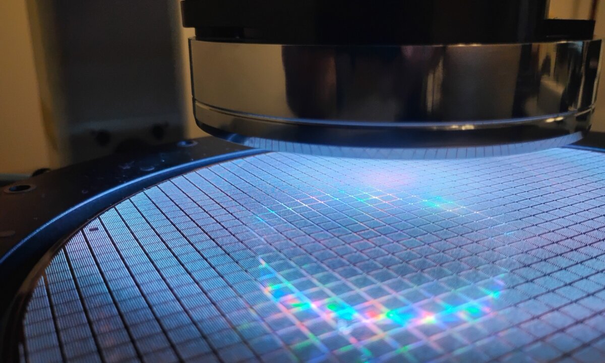
Solder bumps are the tiny balls of solder that connect a semiconductor chip to the circuit board or package it sits on. A single wafer can carry hundreds of thousands of them, and every ball has to be the right size, in the right place, and the right height. Checking them is harder than it sounds. The balls are small and shiny, so many camera systems cannot see the curved top of a ball, and there are far too many balls to measure slowly. This paper explains why wafer bump inspection is difficult, how engineers split the job into flat (2D) and height (3D) measurements, and how VIEW Micro Metrology handles both on a single machine. VIEW uses Continuous Image Capture to check every ball quickly and Area Multi-Focus to measure ball height and coplanarity. A simple wafer example walks through the full process from start to finish.
What a solder bump is, and why inspection matters
A semiconductor chip cannot do anything until it is connected to the outside world. One common way to make those connections is with solder bumps, small balls of solder arranged in a grid on the surface of the chip. When the chip is flipped face down onto matching pads and heated, the balls melt and bond, joining the chip to its package or board. Because the chip is turned upside down, this is called flip-chip assembly, and the grid of balls is called a ball grid array, or BGA. The earliest form of this joint is still known by its older name, C4, short for controlled collapse chip connection.
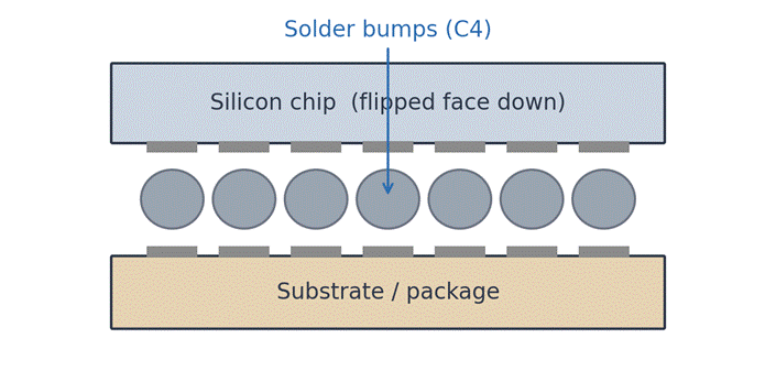
Figure 1. In flip-chip assembly the chip is turned face down and joined to its substrate through an array of solder bumps. The earliest form of this joint is the controlled collapse chip connection, or C4.
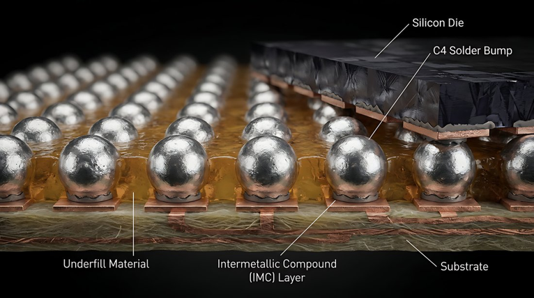
Figure 2. Cross-section of a flip-chip interconnect. Each C4 solder bump joins the silicon die to the substrate through a copper pad and a thin intermetallic compound, or IMC, layer, with underfill surrounding the joints. Optical inspection sees only the outer surface of the bump; IMC formation and interface strength are confirmed by cross-section and reliability testing, not by the camera.
The numbers involved are large. A wafer, the thin disc of silicon that chips are built on, can hold more than a thousand chips, and each chip can carry a hundred or more balls, which adds up to hundreds of thousands of solder balls on one wafer. If even one ball is missing, too small, or too short to reach its pad, that connection can fail and the chip may not work. For that reason manufacturers inspect the balls before the chips move on. Inspection simply means measuring each ball and comparing it against acceptable specifications.
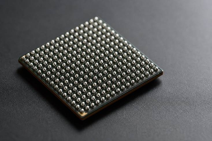
Figure 3. The underside of a ball grid array package. Every bright sphere is a solder ball; a single production wafer multiplies this into hundreds of thousands of them, and each one must be present, correctly sized, and coplanar for the assembly to bond.
One of the most important measurements is coplanarity. Picture lowering a flat sheet of glass onto all of the balls at once. If every ball touches the glass, the balls are coplanar, and all of them should reach their pads during reflow. If some balls sit lower than their neighbors, the glass only rests on the tall ones, and the short balls may never connect. Coplanarity is therefore a measure of how level the tops of the balls are across the whole array, and it is among the properties that most directly predict whether an assembly will bond.
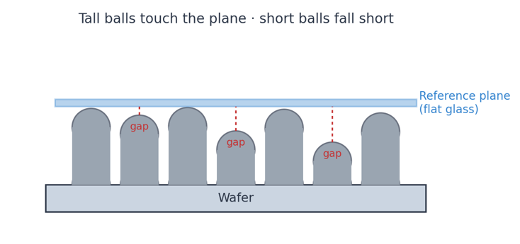
Figure 4. Coplanarity in practice. A flat reference plane lowered onto the array touches only the tallest balls; balls that sit low may never reach their pads during reflow.
Why solder bumps are hard to inspect
A solder ball is one of the hardest things to measure with a camera. It is small, it is round, and its surface is shiny like a tiny mirror. Engineers call a mirror-like surface specular. When light lands on a flat, dull surface it scatters in every direction, and a camera picks it up easily. When light lands on a shiny, curved ball, most of it bounces off at an angle and misses the camera. The very top of the ball, the part that must touch the pad, often shows up as a blinding white spot or a dark hole rather than a surface the system can actually measure.
Figure 5. Why a solder ball is hard to image. Its mirror-like curved surface reflects most light away from the camera, leaving the critical top of the ball as a bright spot or a dark void.
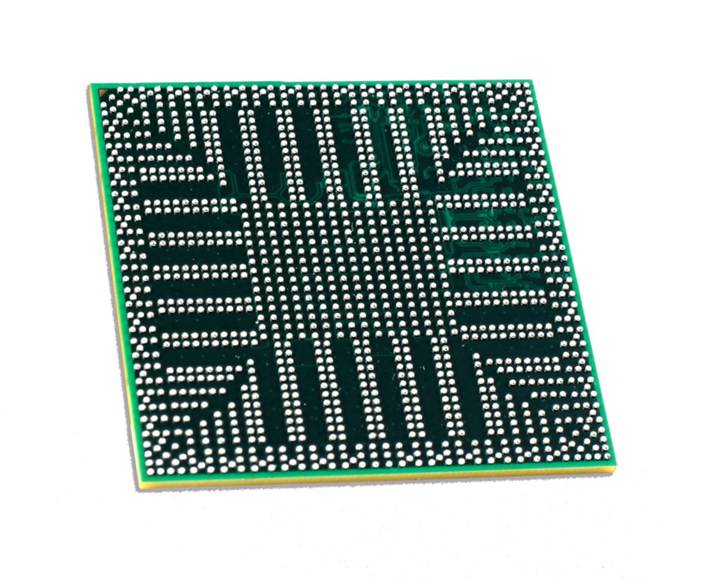
Figure 6. A ball grid array viewed from above. The specular, curved surface of every ball is the core inspection challenge: most light reflects away from the camera, and the ball tops read as blown-out highlights or dark voids rather than measurable surface.
A plain camera looking straight down at the wafer can still do useful work. It can find each ball, confirm that none are missing, and measure how wide each ball looks from above, which is its diameter, and how far apart the balls are, which is called the pitch. What a single top-down camera cannot do is measure height, meaning how tall each ball stands. Height is exactly what coplanarity depends on, so height is the measurement that gives inspection systems the most trouble.
Researchers have invented several ways to measure ball height. One approach, called triangulation, shines a line of light across the balls and watches how that line appears to bend as it climbs over each ball; the size of the bend reveals the height. One such system reported an accuracy of about 1.5 microns, which is roughly one-fiftieth the width of a human hair. Other methods use interferometers, which measure height by comparing light waves, or shadow techniques that calculate height from the length of the shadow a ball casts. Each method balances speed, cost, and level of detail differently, and none of them measures everything at once.
Two kinds of checks: flat (2D) and height (3D)
Because no single tool catches every kind of defect, engineers split the work into two kinds of checks. The first layer is a fast, two-dimensional check, often called automated optical inspection, or AOI. Looking straight down, it confirms that every ball is present and in the right spot, and it measures diameter and pitch. The second layer is a slower, three-dimensional measurement that adds the missing height information, which is then used to calculate coplanarity.
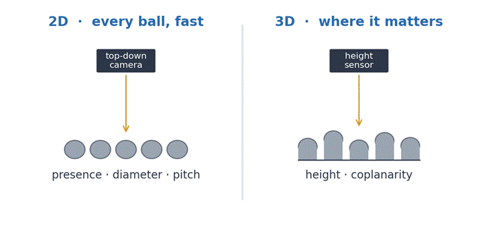
Figure 7. A two-layer inspection strategy. A top-down 2D view screens every ball for presence, diameter and pitch; a slower 3D measurement adds height and coplanarity where they matter.
The order matters because of cost and speed. Modern chips can have so many connections that measuring every single ball in full 3D on every wafer is slower than a high-volume line needs, especially once a fast 2D pass has already cleared most of them. It is also expensive to wait until after a chip is reflowed to discover a bad ball, because by then several good chips stacked or joined with it may have been ruined as well. The practical answer is to screen all of the balls quickly in 2D, then spend the extra 3D measurement time only where height and coplanarity truly matter.
How VIEW sees the top of the ball, and does it quickly
VIEW Micro Metrology builds inspection systems that handle both layers on one machine, and it aims straight at the two hardest problems described above: seeing the shiny top of the ball, and working fast enough to check every ball on a wafer.

Seeing the ball is mostly a lighting problem. Instead of one fixed light, VIEW systems use versatile, programmable illumination together with strong image processing, so the lighting can be tuned until the curved, reflective surface of a ball returns a usable image. For very smooth surfaces that a camera struggles to focus on, a technique called Focus Grid projects a pattern of fine lines onto the part; the system knows it has found the right focus when those projected lines look sharpest. Where more height detail is needed, the systems can also add laser sensors that measure height, depth, and surface shape.
Speed comes from a feature called Continuous Image Capture, or CiC. A traditional system moves to a spot, stops, takes a picture, then moves to the next spot, over and over, and all that stopping and starting wastes time. CiC instead keeps the wafer moving steadily and takes rapid snapshots as it passes beneath the optics, then stitches those snapshots together into one large image. Because the machine never has to stop to take a picture, VIEW states that cycle time is reduced significantly without giving up measurement quality. That speed is what makes it realistic to inspect every ball on a wafer that holds tens of thousands of them.
Measuring height and coplanarity with Area Multi-Focus
To measure height and coplanarity, VIEW uses a technique called Area Multi-Focus, or AMF. Most vision metrology systems already sweep their focus up and down to find the sharpest point on a surface, and that focus sweep quietly contains height information, because any given feature is only in sharp focus at one specific distance from the lens. AMF reuses the data from that normal autofocus step and turns it into a 3D image, which means it does not need a separate, slow scanning motion to build the height map. From that 3D data the system reports height, flatness, roughness, and volume for each feature. To find coplanarity for a whole array, the software builds a height map of all the balls, picks out each ball one by one, and fits a single flat reference plane across the tops of the balls. It then reports how far the balls sit above or below that common plane, which is the coplanarity result.
A working example on a real wafer
VIEW engineers ran this entire process on a real wafer as a demonstration. The wafer was a spare part bought secondhand rather than a customer’s production lot, so the exercise shows what the equipment can do, not a qualified factory result, and no formal statistics are claimed. Even so, the steps mirror how a real inspection line would run.
The routine starts with a fast go/no-go check. A software tool called a blob finder captures the shape of each ball and determines whether any balls are missing. A blob is any distinct region, regular or irregular, that the software forms by connecting neighboring pixels within a chosen brightness range; for each one it reports a location and an area, and it ignores anything too small or too large to be a ball. Each chip on this wafer was supposed to have 110 balls. If a chip does not have all 110, it is marked as bad on a map of the wafer, and the system moves on without wasting time measuring it (Figure 8). Only the chips that pass this check move on to the slower 3D step, which saves a great deal of time across a full wafer.
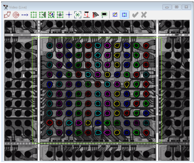
Figure 8. The blob finder acts as a quick pass/fail filter. Colored outlines mark each ball the software detects within the analysis window. If a chip does not show the expected 110 balls, the 3D height sweep is skipped and the system moves to the next chip.
Chips that pass move to the 3D step. An AMF sweep captures the height of the whole ball field. In the resulting image, how bright each point appears corresponds to how tall it is, so brightness is really a height reading in disguise. The software isolates each ball, collects its height values, and uses them to calculate the coplanarity of that array (Figure 9). The same capture also carries the 2D information, so ball diameter, position, and pitch come from the very same measurement, with no second pass needed.
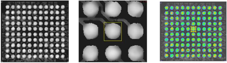
Figure 9. Flat (2D) views of the Area Multi-Focus result. Grayscale intensity represents calculated Z height. The software uses the underlying height data for each ball to calculate coplanarity.
Shown in three dimensions, the height map makes a low or tilted ball easy to spot at a glance (Figure 10). From the individual ball heights, the system can calculate an average and a spread, called the standard deviation, and, if the customer supplies acceptable upper and lower limits, standard quality scores as well. The demonstration also makes a practical point about speed. The quick 2D scan can check an entire wafer for missing and mis-sized balls in a matter of minutes, while the slower, more detailed 3D height sweep is saved only for the coplanarity measurement that truly needs it.
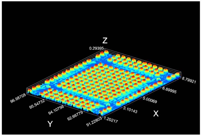
Figure 10. A three-dimensional height map of one ball grid array. Color stands for height, from blue at the base to red at the peak, so a short ball or a tilted array is easy to see at a glance. Axis values are in millimeters.
Where this technology is heading
Solder bump inspection is not fading away; if anything, it is growing. Flip-chip and BGA parts are everywhere, and newer packaging styles reuse the same ideas. Fan-out wafer-level packaging, for example, spreads a chip’s connections out onto a larger rebuilt wafer, and it still needs the same checks for ball height, alignment, and warpage, which is any unwanted bending of the wafer.
Two trends make the measurement harder over time. First, the balls keep shrinking. Very small solder balls are called microbumps, and a related connection called a copper pillar uses a short copper post capped with a little solder to reach even tighter spacing. Measuring these smaller features means switching to higher-magnification lenses, and that brings a trade-off: a stronger lens sees finer detail but covers a smaller area at a time, which slows inspection down. Engineers constantly balance the smallest ball they need to see against how fast they need to go.
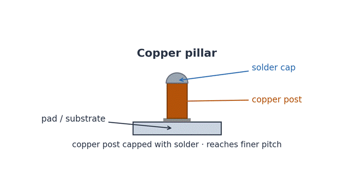
Figure 11. A copper pillar: a short copper post capped with solder. This geometry reaches finer pitch than a conventional solder bump and adds sidewalls and a separate cap that the inspection system must resolve.
Second, a newer method called hybrid bonding is starting to appear at the very finest spacings. Instead of using a solder ball, it joins copper directly to copper. Hybrid bonding is a separate, longer-term technology, and it will not necessarily replace the enormous number of solder-bumped and wire-bonded chips that make up most of what ships today, but it is worth watching as connections continue to shrink. It is also worth remembering that a camera only ever sees the outside of a ball. Whether the joint is genuinely strong is confirmed later with separate strength and reliability tests, not by optical measurement alone.
Conclusion
Wafer bump inspection comes down to a simple truth with hard consequences. The interconnects that make a chip work are small, shiny, and present by the hundreds of thousands, and they can fail in more ways than a camera can see. Optically, the defects fall into two groups: a ball can be in the wrong place, missing, undersized, bridged, or shifted off its pad, or it can be the wrong height, sitting too low to reach the pad it is meant to join. A joint can also fail internally or electrically, in ways optical inspection cannot detect, which is why shear, cross-section, and electrical testing remain part of a complete quality plan. The first kind of defect is a two-dimensional problem that a fast top-down check catches efficiently. The second is a three-dimensional problem that only a height measurement can resolve, and it drives coplanarity, a property that strongly predicts whether an assembly will bond. Any inspection plan that controls only one of these failure modes leaves the other free to reach the customer.
The practical answer is a layered strategy carried out on a single platform. Two-dimensional automated optical inspection screens every ball on every wafer for presence, diameter, pitch, and bridging, quickly enough to keep pace with production. Three-dimensional metrology then measures height and coplanarity where those parameters decide yield, without forcing a full volumetric scan of features that a fast image has already cleared. VIEW Micro Metrology builds both layers into one system. Programmable illumination and strong image processing recover a usable signal from the curved, specular top of a ball, Continuous Image Capture keeps the wafer moving so cycle time stays compatible with volume, and Area Multi-Focus reuses the tool’s own focus sweep to report height, flatness, roughness, and volume without a separate scanning motion. Consolidating both layers on one machine removes a handoff, shortens cycle time, and lets inspection move upstream, where catching a defect before reflow or bonding is far cheaper than discovering it after good die have been committed to a stack.
None of this pressure is easing. Balls continue to shrink toward microbumps and copper pillars, fan-out and 2.5D and 3D packaging multiply the number of interconnects per part, and hybrid bonding is beginning to appear at the finest pitches. Each step raises the resolution the measurement must deliver while the count of features to measure keeps climbing, and optical inspection remains the fastest way to screen them in volume, though the finest features increasingly push past what light alone can resolve and call for complementary sensors. It will not answer every question, because a camera sees only the outside of a joint and metallurgical integrity still belongs to shear, cross-section, and reliability testing, but it remains the front line of wafer-level quality. For an engineer whose current system cannot see the tops of the balls, or cannot measure them fast enough to inspect at volume, the message of this paper is direct. The techniques that solve both problems on one platform exist today, and adopting them is a matter of choosing the right tool, not waiting for one to be invented.