
AI accelerators and data‑center GPUs are using memory faster than the industry can add capacity. IEEE Spectrum has said that high‑bandwidth memory is one of the bottlenecks of the AI build‑out [1], [2]. Reuters have reported that AI demand is driving memory shortages and price increases [3], [4]. Micron and SK hynix have both publicly said that AI customers now come first in supply allocation [5], [6]. Whatever the exact numbers look like next quarter, the direction is clear: for the foreseeable future memory is a constrained input.
The answer is to build. New fabs are being built in the United States, Korea, Japan and Taiwan. A memory fab takes years from the first stone to full production and the chips that AI data centers need this year and next will come from lines that already exist.
That leaves a supply line that gets far less attention: the gap between the memory that is made and the memory that reaches a customer. Closing that gap is the job of test, repair and reliability engineering. It can add real capacity in months rather than years.
Where does fabricated memory leak away?
Imagine a pipe with holes in it. Bits are fabricated, tested, shipped, and then put in a server. At two places along the way, memory that was paid for fails: during testing, when silicon dies are scrapped and, in the field, when modules fail and return. Any bits recovered at those two points are bits that did not require a new fabrication.
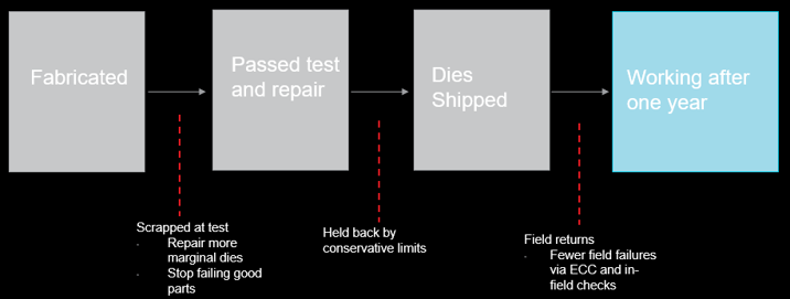
Figure 2 The two leak points and the three levers that plug them
Turning more marginal dies into good ones
No memory die leaves the production line intact. Every contemporary memory contains spare rows and spare columns, and a built-in self-test that locates the damaged cells and replaces them with spares before it even leaves the factory. A die that is fit to sell can be determined largely by the quality of that repair step.
More than most people in the test floor appreciate, the choice of the repair is what makes the difference. A basic plan of substitution may abandon a die that a cleverer plan could repair, because the same spare might be used to repair many faults, if it is used in the right order. Improving that logic requires no silicon, and no new tools. This turn dies that were already paid for into a product.
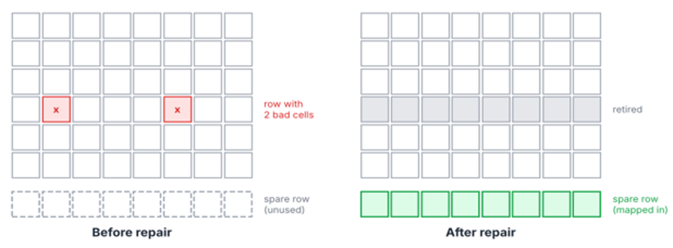
Figure 3 Repair in action: a spare row is mapped for a row with defective cells [8], [9]
Stop throwing away good parts
The test limits are set conservatively due to the high cost associated with delivering a faulty part to the customer. However, by setting limits conservatively we end up rejecting parts that are perfectly good and will work for their life cycle. This is called overkill within the industry and in a competitive market we are losing capacity to the bin.
Overkill comes from two main areas. Firstly, the testing itself. By using aggressive on the fly patterns parts can suffer from temporary voltage drop on the die causing failure unrelated to the memory cells. Secondly, the guard band is often set many years ago for an older process or application. Test flows which take into consideration stress caused during testing and use real data from the field to set test limits will bring back a significant amount of these parts.
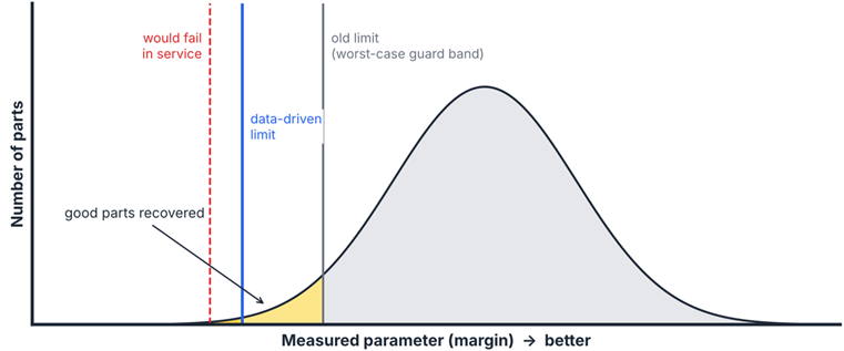
Figure 4 Overkill: parts between the true failure boundary and a stale test limit are good parts thrown away [10], [11]
Keep shipped memory working
Every module that returns from use goes through two rounds of consumption: first when it is manufactured, and second during its replacement. A field failure directly impacts supply and therefore reducing field failures is as much about capability as it is about quality.
Some of the available techniques will do the heavy lifting here. Error correcting codes that are used in the die and in the controller will help catch and fix bit errors before they can cause system failures. Tests for reliable operation, including the tests that are performed regularly while the module is idle in the field, will help catch defective devices before things go so bad that they would need to be thrown away for good.
Same techniques, different memories
The three levers work everywhere, but each has its sweet spot. Embedded SRAM is packaged within a logic chip. That means its yield is coupled to that host chip’s yield, and a low-cost repair step can salvage an otherwise pricey processor. Standalone DRAM has the most mature repair/screening flows and the most reliability field data, so naturally reliability-aware test limits are the most developed in that market. HBM stacks multiple DRAM dies vertically, so a failing die can ruin an entire stack. Repair, and die-level screening, are the biggest lever you have on HBM supply. Newer memories like MRAM and RRAM are still developing the repair methodologies and reliability field-history database DRAM starts with.
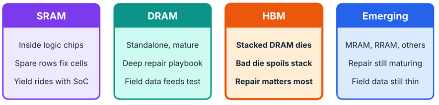
Figure 5 How test, repair, and reliability levers play out across SRAM, DRAM, HBM, and emerging memories
None of these changes the need for new fabs. The future solution to the growing demand for AI memory is the need for increased production of wafers, which is exactly what the industry is in the process of delivering. However, the next two years will be defined by how much useful memory comes out from the existing production lines, which cannot be established in advance. It changes with every repair improvement, with every additional piece returned to usability, and with every failure of a field that has been avoided.
The conclusion for the suppliers of memory is that the testing stage should be implemented with similar investments to that of the fabrication plant. For memory purchasing companies, the important ask to suppliers is not just how many wafers they are going to start producing, but how many of those will be shipped to the customer and whether they will be safe for using.
REFERENCES
[1] S. K. Moore, “How and When the Memory Chip Shortage Will End,” IEEE Spectrum, 10 Feb. 2026 (updated Apr. 2026). https://spectrum.ieee.org/dram-shortage
[2] H. Goldstein, “AI Is Insatiable,” IEEE Spectrum, 6 Apr. 2026. https://spectrum.ieee.org/high-bandwidth-memory-shortage

[3] M. A. Cherney et al., “The AI frenzy is driving a new global supply chain crisis,” Reuters, 2 Dec. 2025. Syndicated copy: https://www.investing.com/news/stock-market-news/the-ai-frenzy-is-driving-a-new-global-supply-chain-crisis-4387303
[4] Reuters, “TrendForce sees chip prices surging 90-95% in Q1 from previous quarter,” 2 Feb. 2026. https://www.reuters.com/technology/trendforce-sees-chip-prices-surging-90-95-q1-previous-quarter-2026-02-02/
[5] Micron Technology, “Micron Announces Exit from Crucial Consumer Business,” press release, Boise, ID, 3 Dec. 2025. https://investors.micron.com/news-releases/news-release-details/micron-announces-exit-crucial-consumer-business
[6] SK hynix, “SK hynix Announces 3Q25 Financial Results,” press release, 29 Oct. 2025 (2026 DRAM, NAND and HBM supply discussions with customers completed; capacity reported sold out on the earnings call). https://www.prnewswire.com/news-releases/sk-hynix-announces-3q25-financial-results-302597593.html
[7] “Why Memory is Considered the Backbone of AI, Cloud & Data Centres,” LinkedIn. https://www.linkedin.com/pulse/why-memory-considered-backbone-ai-cloud-data-centres-ezsqc Figure 1 Memory: Backbone of AI, Cloud & Data Centers [7]
[8] J.-F. Li, J.-C. Yeh, R.-F. Huang, and C.-W. Wu, “A built-in self-repair design for RAMs with 2-D redundancy,” IEEE Trans. VLSI Systems, vol. 13, no. 6, pp. 742-745, Jun. 2005. https://doi.org/10.1109/TVLSI.2005.848824
[9] T.-W. Tseng and J.-F. Li, “A low-cost built-in redundancy-analysis scheme for word-oriented RAMs with 2-D redundancy,” IEEE Trans. VLSI Systems, vol. 19, no. 11, pp. 1983-1995, Nov. 2011. https://doi.org/10.1109/TVLSI.2010.2066587
[10] N. Neethirajan et al., “Overkill reduction using inter-test correlation of customer-promised and non-customer-promised tests,” SRC TECHCON, 2021. https://personal.utdallas.edu/~yiorgos.makris/papers/techcon21.pdf
[11] L. Kapitza et al., “Quality control of lifetime drift in discrete electrical parameters in semiconductor devices via transition modeling,” arXiv:2501.07115, 2025. https://arxiv.org/abs/2501.07115
Author Bio –
Sriram Nithin Gopal Lanka is a Senior Product Development Engineer at Advanced Micro
Devices, Inc. (AMD) in Austin Texas where he has worked on DFT scan testing, memory BIST,
Diagnostics, leakage testing, array repair, bitmapping, new product characterization, yield
improvement and test program ownership at wafer sort and final test, and test time reduction.
Before joining AMD, he was a research and development failure analysis intern at NXP
Semiconductors in Austin, where he performed electrical fault isolation for new product
introduction, qualification, yield enhancement and customer quality complaints. He also worked
as design and validation co-op at Skyworks Solutions in Irvine CA on RF power amplifier design
and measurement. He holds an M.S. in Electrical Engineering from Iowa State University. His
interests are silicon debug, yield learning and closer collaboration between production test and
failure analysis. He serves on the technical peer-review committees of IEEE and other
international conferences in tests, reliability, and packaging.