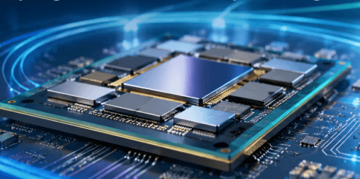
The next phase of AI infrastructure development will depend on more than faster processors. As computing systems expand to accommodate increasingly demanding workloads, the connections between processors, accelerators, memory, and networking equipment are becoming an important engineering consideration. This is bringing silicon photonics and co-packaged optics (CPO) closer to the centre of semiconductor packaging and data centre design.
Traditional optical networking relies on transceivers installed separately from the switch or processor package. Electrical signals travel through the electronic system before reaching these modules, where they are converted into optical signals for transmission over fibre. Although this arrangement offers flexibility in maintenance and upgrades, the increasing demands of AI infrastructure are creating pressure to reduce electrical transmission distances and improve the efficiency of high-bandwidth connections.
CPO addresses this challenge by bringing optical engines closer to switching or computing silicon. However, integrating optical and electronic components within a common package introduces manufacturing requirements that extend beyond chip design. Optical alignment, thermal stability, testing, assembly yield, and serviceability all become important considerations.
The central manufacturing question is no longer simply how much bandwidth an optical device can support. It is whether the complete photonic-electronic assembly can deliver that performance consistently at production scale.
The North American Photonic Integrated Circuit Market Reflects the Broader Shift
The commercial push behind integrated photonics is undeniable. In our team’s latest research at Vyansa Intelligence, the North America Photonic Integrated Circuit Market Report, we project the regional market will climb from USD 8.29 billion in 2026 to USD 13.29 billion by 2032, maintaining an 8.18% compound annual growth rate.
Data centers make up the core of this demand. They represent 36% of the 2026 total, or roughly USD 2.98 billion.
These figures tell an important story: demand for optical silicon is real. But CPO will not replace pluggable transceivers overnight. Traditional pluggables will keep enterprise data centers for years because field technicians can swap them in seconds. CPO belongs where thermal limits leave engineers no other choice: hyperscale AI training clusters.
The distinction matters because CPO represents a change in system architecture rather than a complete replacement of existing optical technologies. Conventional transceivers will continue to serve applications where modularity and field replacement are important. CPO is more relevant to systems in which bandwidth density, electrical reach, and power efficiency justify closer integration.
Market forecasts therefore provide an indication of the expanding photonics ecosystem, while actual CPO adoption will depend on application-specific economics, manufacturing readiness, and system requirements.
Why Optical Conversion Is Moving Closer to Computing Silicon
As data rates increase, electrical signals become more difficult to transmit over longer distances without additional signal conditioning. Losses in electrical channels, equalisation requirements, routing constraints, and power consumption can affect the design of high-speed interconnects.
Placing optical conversion closer to the source of the signal can reduce the electrical distance between the processor or switch ASIC and the optical interface. This can help address some of the limitations associated with conventional interconnects, although the overall benefit depends on the complete system design.
The commercial opportunity lies in improving connectivity without allowing the interconnect itself to become a disproportionate source of power consumption, complexity, or performance constraints.
Two developments illustrate how suppliers are approaching this requirement.
In May 2026, GlobalFoundries announced its SCALE co-packaged optics solution. The platform uses silicon photonics and supports coarse wavelength-division multiplexing (CWDM) and dense wavelength-division multiplexing (DWDM), enabling bidirectional transmission over optical fibre. GlobalFoundries positioned the platform for AI scale-up architectures and identified its compatibility with the Optical Compute Interconnect Multi-Source Agreement (OCI MSA).
In January 2026, NVIDIA described its Spectrum-X Ethernet Photonics networking platform, including the SN6800 switch, which supports an aggregate bandwidth of 409.6 Tb/s. The architecture incorporates co-packaged silicon photonics and is designed for large-scale AI networking.
These developments demonstrate that optical integration is advancing beyond incremental improvements to standalone transceivers. Semiconductor manufacturers and networking suppliers are developing architectures in which optical connectivity is considered alongside switching silicon, package design, and system-level performance.
The implication for manufacturers is significant: optical engines must be designed not only to meet optical specifications but also to integrate with the mechanical, electrical, and thermal requirements of the host package.
CPO Changes the Economics of Optical Integration
Conventional pluggable transceivers provide a practical separation between optical components and the host system. Operators can replace a failed module, qualify a new transceiver independently, or upgrade connectivity without necessarily replacing the switch package.
CPO changes this relationship by moving optical functionality closer to the main electronic components. The resulting architecture can improve integration and reduce the length of high-speed electrical connections, but it also changes the consequences of manufacturing defects and component failures.
For example, a defect identified in a standalone transceiver can often be addressed by replacing the module. If an optical engine is integrated into a more complex package, the same failure may require a more involved repair or replacement process, depending on the architecture.
This creates a manufacturing trade-off. Tighter integration may deliver system-level benefits, but those benefits must be evaluated against assembly complexity, repairability, and the cost of rejected components.
Intel’s optical input/output (I/O) chiplet development provides another example of the move towards closer integration. In a demonstration announced in 2024, Intel reported bidirectional bandwidth of up to 4 Tb/s. The chiplet was designed to support optical connectivity between computing platforms, with applications extending to CPUs, GPUs, infrastructure processing units, and other systems-on-chip.
Intel also reported that the demonstrated optical link consumed approximately 5 picojoules per bit, compared with approximately 15 picojoules per bit for the pluggable optical transceiver modules used as its comparison.
These figures relate to Intel’s reported demonstration and should not be treated as universal performance values for every CPO architecture. Nevertheless, they illustrate why the industry is investigating optical connectivity as part of the computing package rather than treating it exclusively as a networking component.
Optical Alignment Is Becoming a Production-Critical Process
One of the most important differences between conventional electronic assembly and photonic packaging is the need to establish a reliable optical path between components.
Electrical connections can often accommodate certain mechanical variations through established interconnect structures. Optical coupling, by contrast, depends on the position and characteristics of the waveguides, fibres, and couplers involved. Misalignment can increase optical losses and reduce the amount of light transferred through the intended path.
This makes alignment accuracy a direct contributor to manufacturing performance.
Research published by imec on high-density CPO interfaces examined a silicon nitride (SiN) taper connected through an optical redistribution layer. The demonstrated structure achieved a reported 1 dB lateral misalignment tolerance of approximately ±1.8 micrometres.
The result illustrates the precision that can be required at the optical interface. It should not be interpreted as a universal tolerance for all photonic packages, because acceptable alignment depends on the coupling design, materials, geometry, and optical specifications.
Manufacturers can approach this challenge through active or passive alignment.
Active alignment uses optical measurements to guide component positioning before attachment. Passive alignment relies on engineered mechanical references, fiducials, grooves, or other precision structures to establish the required position.
The choice affects equipment requirements, assembly time, process complexity, and repeatability. Active alignment can provide direct feedback on optical performance, while passive approaches can support more repeatable assembly when the mechanical design and process controls are sufficiently mature.
The more important question is how reliably the chosen approach performs across production lots and operating conditions.
A prototype that achieves excellent optical coupling under controlled laboratory conditions does not automatically establish a process suitable for high-volume manufacturing. Production equipment must reproduce the alignment, bonding, and attachment process consistently while maintaining throughput and traceability.
Testing Must Move Earlier in the Manufacturing Process
Testing is another area in which photonic integration changes established semiconductor manufacturing practices.
Traditional semiconductor test flows concentrate heavily on electrical measurements. Silicon photonics requires additional optical measurements to evaluate parameters such as coupling efficiency, optical power, modulation performance, and the behaviour of integrated photonic components.
Testing only after the final package has been assembled can expose manufacturers to avoidable costs. By that stage, a device may already contain several integrated components and may have undergone multiple assembly operations. A defect discovered late in the process can therefore result in the loss of more manufacturing value than a defect identified earlier.
A practical manufacturing strategy involves testing at multiple stages:
- Wafer-level testing: Identify defective photonic devices before singulation and downstream assembly.
- Die-level testing: Evaluate individual components before integrating them into a more complex assembly.
- Optical-engine testing: Assess the interaction between photonic devices and their associated electrical components.
- Package-level testing: Verify optical, electrical, and thermal performance after assembly.
- Reliability testing: Establish whether performance remains stable under specified operating and environmental conditions.
This approach does not eliminate the need for final testing. Instead, it distributes quality control throughout the manufacturing flow, allowing defects to be detected closer to the process stage where they originate.
A June 2026 announcement by Advantest and OpenLight provides evidence of the industry’s focus on this issue. The companies announced a collaboration to develop silicon-photonics testing solutions for scalable, high-volume manufacturing, with particular attention to electro-optical devices and optical engines.
The development is relevant because manufacturing capacity depends on more than wafer fabrication. Equipment must also support repeatable optical access, automated handling, and sufficiently efficient testing to avoid creating a bottleneck between fabrication and final assembly.

For CPO manufacturers, the commercial objective is to establish a test strategy that identifies defects early without making inspection so slow or expensive that it undermines production economics.
Thermal Management Must Be Designed Alongside the Optical Package
Bringing optical engines closer to high-performance processors and switching ASICs creates a shared thermal environment. This introduces a challenge that cannot be addressed solely through conventional optical-device design.
Processors and switch ASICs generate heat during operation. Photonic components and laser sources also have temperature-dependent operating characteristics. Changes in temperature can affect optical output, wavelength stability, and the performance of certain photonic structures.
Thermal expansion introduces an additional consideration. Package materials may expand at different rates, potentially changing the relative positions of optical interfaces or increasing mechanical stress during temperature cycling.
These effects are not identical across all designs, but they demonstrate why optical performance and package reliability must be evaluated together.
The implications extend to the placement of laser sources, the selection of package materials, the design of cooling structures, and the management of heat generated by neighbouring electronic components.
NVIDIA’s Quantum-X800 InfiniBand photonics switch, announced as part of its 2026 networking developments, incorporates liquid cooling alongside silicon-photonics connectivity. The platform illustrates how thermal management is being considered within the broader networking architecture.
However, the use of liquid cooling in a particular platform does not establish that every CPO system requires the same approach. Cooling requirements depend on component power, package density, system configuration, and operating conditions.
The broader manufacturing lesson is that thermal constraints need to be established early in package development. If optical placement, mechanical attachment, and cooling are designed independently, later integration can require costly changes to the package or assembly process.
Mixed-Material Packaging Is Expanding the Manufacturing Challenge
A CPO assembly may combine silicon photonic integrated circuits, electronic driver and receiver chips, laser sources, fibre arrays, optical connectors, interposers, redistribution layers, and thermal-management structures.
These components do not necessarily share the same manufacturing processes or material requirements. Their integration requires control over placement, bonding, electrical connectivity, optical coupling, and mechanical stability.
The resulting challenge spans several stages of the semiconductor supply chain.
Wafer fabrication must produce photonic devices that meet their design specifications. Packaging operations must integrate those devices with electronic components. Optical assembly must establish reliable coupling, while test processes must verify the combined system.
A weakness at any stage can affect the yield or reliability of the final product.
GlobalFoundries’ silicon-photonics manufacturing portfolio illustrates the breadth of capabilities being developed around this requirement. The company combines silicon-photonics fabrication with packaging and testing capabilities and has described support for different fibre-attachment approaches.
These capabilities matter because the commercialisation of CPO depends on coordination between semiconductor fabrication, optical assembly, and final package integration. A supplier that can manufacture a high-performing photonic die may still require additional capabilities or partners to deliver a complete, production-ready optical subsystem.
This also creates opportunities for specialised packaging and test providers. As more optical functionality enters semiconductor packages, demand can extend beyond photonic chip fabrication to precision assembly, optical inspection, interconnection, and reliability qualification.
The opportunity, however, depends on whether these services can be delivered with consistent quality and commercially viable throughput.
Investment Is Shifting Towards Manufacturing Readiness
Investment activity provides another indication that the industry is moving from component development towards production preparation.
On 10 September 2026, Ayar Labs announced an additional USD 150 million in funding, bringing its reported primary capital raised during 2026 to USD 650 million. The company stated that the funding would support product development, validation, manufacturing ecosystem readiness, and the transition towards high-volume production. It also announced plans for a new design centre in Bengaluru, India.
The significance of this announcement lies in the range of activities the funding is intended to support. Commercialising CPO requires more than developing a photonic device. It also involves validating the product, preparing the manufacturing ecosystem, coordinating with suppliers, and establishing the capabilities needed to support customer programmes.
Funding alone does not demonstrate that a manufacturer has achieved high-volume production or commercially competitive yields. It does, however, show that manufacturing readiness is an explicit part of the development strategy.
For the broader supply chain, this creates potential opportunities in optical packaging, testing equipment, semiconductor integration, and engineering services. It may also increase the importance of manufacturing partners that can support the transition from initial validation to repeatable production.
What Will Determine the Commercial Scalability of CPO?
The transition to CPO is creating a more integrated relationship between photonic design and semiconductor manufacturing. Its commercial success will depend on whether that integration produces measurable system-level benefits without introducing disproportionate manufacturing costs or operational complexity.
Five factors deserve particular attention.
First, manufacturing yield. As optical, electrical, and mechanical components are integrated, defects at different stages can affect the final assembly. Identifying and isolating these defects early will be important for controlling production costs.
Second, alignment repeatability. Optical coupling must remain within the tolerances required by the selected architecture. Production equipment and assembly processes must reproduce these conditions consistently rather than relying on isolated successful demonstrations.
Third, thermal and mechanical reliability. Photonic components must operate within their specified conditions while sharing a package with heat-generating electronic devices. Reliability validation must account for the combined effects of temperature, materials, and mechanical interfaces.
Fourth, test economics. Optical testing must provide sufficient coverage without creating an unacceptable constraint on production throughput. The balance between early defect detection, equipment investment, and test time will influence the economics of manufacturing.
Fifth, serviceability. Tighter integration can make individual component replacement more difficult. The choice between detachable optical interfaces and more permanent attachment will therefore depend partly on the operational requirements of the intended application.
These factors are interconnected. A packaging architecture that improves bandwidth density but proves difficult to assemble or test may not deliver the expected commercial advantage. Similarly, a design that performs well initially may face adoption challenges if thermal cycling, maintenance requirements, or production variability undermine reliability.
The companies best positioned to commercialise CPO will therefore need to demonstrate performance across the complete manufacturing process, not only at the photonic-device level.
Conclusion: The Package Is Becoming the Critical Point of Integration
Silicon photonics and CPO are changing the way optical connectivity is designed and manufactured for AI infrastructure and high-performance computing. The move towards closer integration can reduce electrical transmission distances and support higher-bandwidth architectures, but it also brings optical alignment, thermal management, testing, and assembly into the semiconductor packaging process.
Developments from GlobalFoundries, NVIDIA, Intel, Advantest, OpenLight, and Ayar Labs demonstrate activity across different parts of this ecosystem, from photonic integration and networking platforms to testing and manufacturing readiness.
The next stage of progress will depend on converting these technical capabilities into repeatable production processes. Manufacturers must control optical coupling, identify defects early, manage the interaction between photonic and electronic components, and establish reliable assembly and testing methods.
The commercial significance of CPO will ultimately depend on whether these requirements can be met at the scale, cost, and reliability demanded by AI infrastructure.
For the semiconductor industry, this makes the package more than a physical enclosure for integrated components. It is becoming the point at which optical performance, electrical design, thermal engineering, and manufacturing economics converge.
Author Bio
Pooja Dhoundiyal is a Research Manager at Vyansa Intelligence with an engineering background and more than nine years of experience in market research. Her areas of expertise include semiconductor packaging, microelectronics, and emerging semiconductor technologies. She leads research initiatives examining technology developments, industry dynamics, and evolving requirements across the semiconductor ecosystem.