
Continuing our look at the 2021 IMAPS International Symposium, let’s take a deeper look at the integrated photonics keynote presentation by Tyndall Institute.
Integrated Photonics at Tyndall Institute
Peter O’Brien discussed “Packaging Technologies for Integrated Photonics”. Tyndall Institute is part of Univ College Cork Ireland. They offer prototyping platforms and on-site photonics training funded by the European Commission.
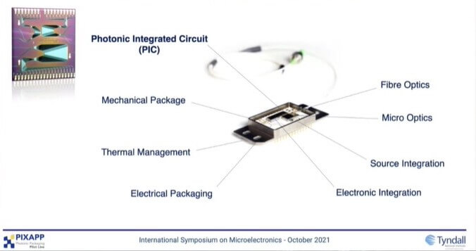
Photonic integrated circuits (PICS) are getting more complex. There are greater demands on thermal management since photonic devices are extremely sensitive to thermal shifts. There is also a move towards more wafer-level packaging (WLP). Photonic packaging technologies are shown in Figure 1. Packaging is responsible for 50-75% of overall photonics costs.
There are reportedly no package designs that allow you to optimize all these factors at once. Today’s photonics packages are generally custom and difficult to scale.
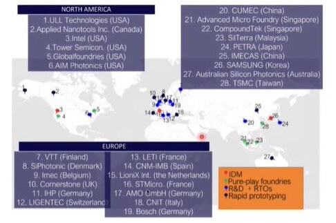
Key players across the globe are listed below. Data centers are key to driving the market.
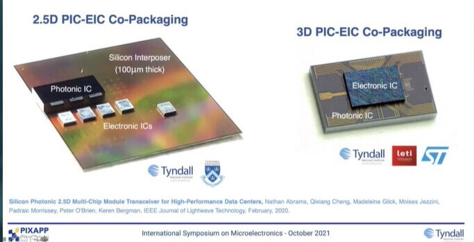
Optical/electrical co-packaging can be accomplished either on an interposer or a direct stack as shown in Figure 3. The stacking can cause temperature rises, which is not compatible with temperature-sensitive photonic devices.
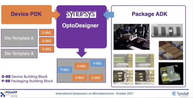
Tyndall is working with Synopsys to develop standard photonic packaging design rules to try to standardize photonics packaging (Figure 4).
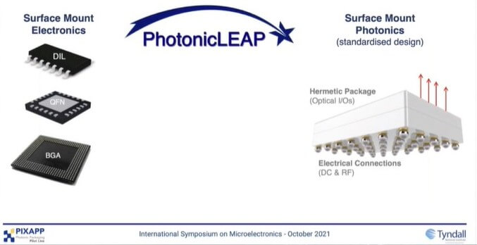
Tyndall is also working on the new European project, Photonic LEAP to create surface mount photonics using glass interposer technology. This is proposed to allow for wafer-level assembly (Figure 5).
IEEE EPS Webinars
One of the benefits available through the IEEE Electronic Packaging Society (EPS) is the available webinars. You can check them out here.

Take special notice of the individual webinars on the different chapters of the Heterogeneous Integration Roadmap. They are worth a listen. Access is free for all IEEE members.
TSMC / Sony JV
Taipai Times reports that TSMC and Sony Semiconductor have announced plans to set up a joint venture — Japan Advanced Semiconductor Manufacturing Inc (JASM) — to build a semiconductor fab in Japan’s Kumamoto Prefecture that would initially produce 22-nanometer and 28-nanometer chips.
Sony commented, “While the global semiconductor shortage is expected to be prolonged, we expect the partnership with TSMC to contribute to securing a stable supply of logic wafers, not only for us but also for the overall industry.”
The capital expenditure is estimated to be ~ $7 billion, with strong support from the Japanese government. TSMC’s board approved investment up to $2.12B that would give it a majority shareholding in the planned venture. Sony Semiconductor, a subsidiary of Sony Corp, will invest $500 MM in JASM, giving it ~ 20 percent ownership. Construction is scheduled for the 2022 year, with production expected in 2024. The fab is expected to have a monthly production capacity of 45,000 12-inch wafers.
For all the latest in Advanced Packaging stay linked to IFTLE………………………………..


