
As technology rapidly moves forward, the reduction of device and chip size is playing an important role in implementing as many chips and sensors in the smallest space. For this reason, the thickness reduction of semiconductor wafers is necessary. Thin semiconductor wafers (thickness around 50-100 µm) are flexible and fragile. Temporary mechanical stabilization is needed to enable processing the device wafer and further decrease device wafer thickness. This involves temporarily bonding device wafers to the carrier. Carrier wafers are used for mechanical and handling support throughout processing and can be detached after using one of the following different de-bonding technologies.
Carrier Wafers for Chemical Release
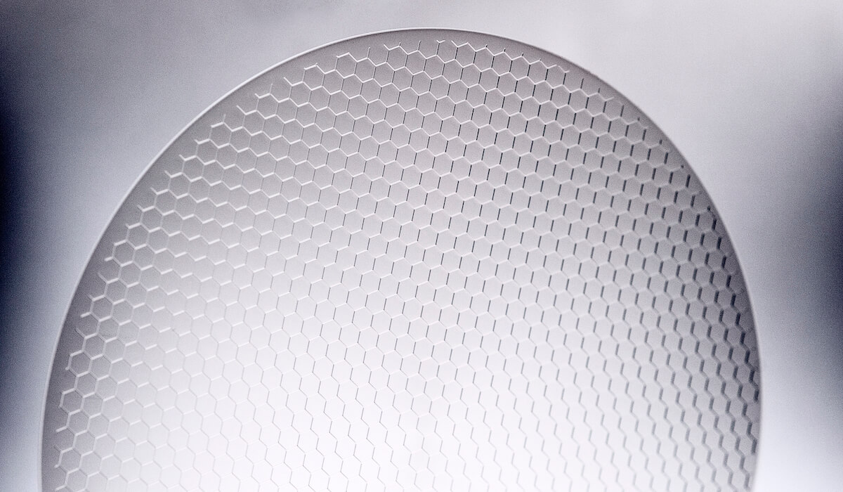
During a chemical release process, a solvent gets in contact with the adhesive and releases it. For this type of de-bonding, thousands of through holes through the carrier wafer are needed to provide consistent contact and fast decomposition of the adhesive (Figure 1).
Carrier Wafers for Laser Release
After processing, the adhesive interlayer will be exposed by using a laser. After exposure, the interlayer will lose its adhesion and the device and carrier wafers can be separated.
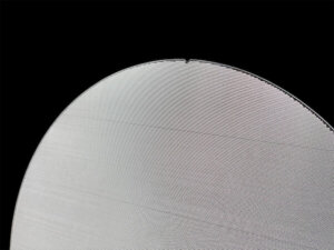
Carrier Wafers Thermal Release
By heating up the processed wafer stack, the adhesive interlayer loses its adhesion and the device wafer can be released from the carrier by a so-called shear or slide-off de-bond (Figure 2).
Glass is used as carrier wafer material due to its mechanical stability and chemical resistance. Matching the coefficient of thermal expansion (CTE) to the device wafer substrate material – for example, silicon, gallium arsenide, indium phosphide, or silicon carbide – is critical to reducing the risk of wafer bow or warp. CTE can be adjusted by using different types of glass.
Additionally, the transparency of glass is not only used for laser de-bonding process but furthermore for in-process inspection. Also, laser markings or QR-codes can be implemented for process traceability.
Plan Optik offers the plain carrier (excluding the adhesives) but is closely co-operating with adhesive and equipment makers. All Plan Optik carrier wafers can be reused up to 30 times (depending on the details of the used process).

Off-the-shelf Carriers for Thin Wafer Handling
Due to an increased demand for fastidious carriers available in short lead times, Wafer Universe is now providing carriers with common specifications off the shelf. These are specially made for laser and mechanical de-bonding processes.
The CTE of the used materials is adapted to silicon or gallium arsenide. Different grades of total thickness variation (TTV) (down to < 1µm) and thickness tolerances (down to ±3 µm) enable a smooth integration in running productions.
All carriers are available for various wafer diameters (150mm, 200mm, 300mm) off the shelf with a lead time of less than one week.
If you are interested to learn more about carriers for temporary bonding and de-bonding and how these carriers can be applied to your thin wafer handling process, please contact us!
