The semiconductor industry’s decades-long adherence to Moore’s Law doctrine of doubling transistor counts on monolithic devices every 18 – 24 months has been amazingly successful. It’s now possible to integrate tens of billions of transistors onto a monolithic die whose area may be hundreds of square millimeters. The resulting chips provide massive amounts of horsepower for current applications such as high-performance computing, machine learning, graphics, and gaming; as well as for emerging opportunities such as implementing the metaverse.
However, the rising costs of designing and building chips on leading-edge processes limit access to the technology. Although the demand for functional integration continues to grow as more markets take up the advantages of electronics and system designs become more diverse, many applications cannot make an economic case for pure monolithic integration. Another way must be found to ensure that the considerable advantages of integration remain widely available.
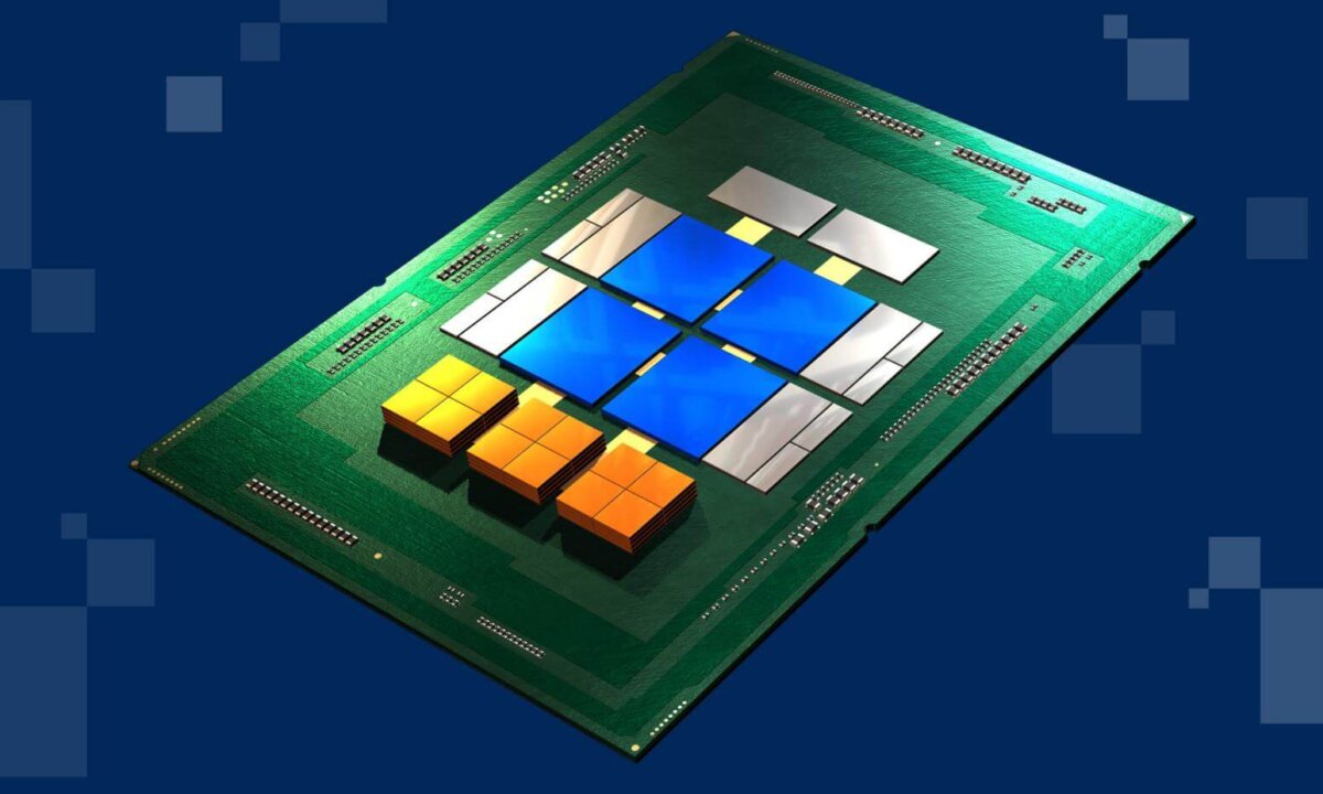
IC packaging innovation tends to move hand-in-hand with IC process development. The latest step along this path is the development of ‘chiplets’: Bare dies that carry a particular function and have an electrical interface that enables them to be interconnected using silicon interposers and assembled into 3D systems-in-packages (SIPs) (Figure 1).
There are many advantages to this approach. The first is that it can create much greater functional densities than could be achieved using packaged chips connected with a PCB, or even package-on-package techniques. The second is that it enables designers to choose the right process for the functionality. Designing analog and mixed-signal circuitry that works consistently on leading-edge processes across all process corners are hard. This ability to match functionality to process can also lead to higher performance. Think of the advantages of putting RF circuitry on a high-frequency process rather than vanilla CMOS.
Perhaps the most intriguing opportunity of a shift to chiplet-based designs is that it could spur the development of a market for chiplets carrying standard functions, such as high-speed I/O or analog-to-digital converters. Designers could then assemble their choice of such chiplets to produce highly optimized 3D SIPs—achieving SoC-like integration and performance much more quickly and cost-effectively than would be possible by attempting the monolithic route—if that was even an economically viable option.
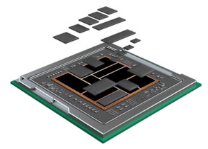
However, the development of a chiplet ecosystem comes with technical and business challenges (Figure 2).
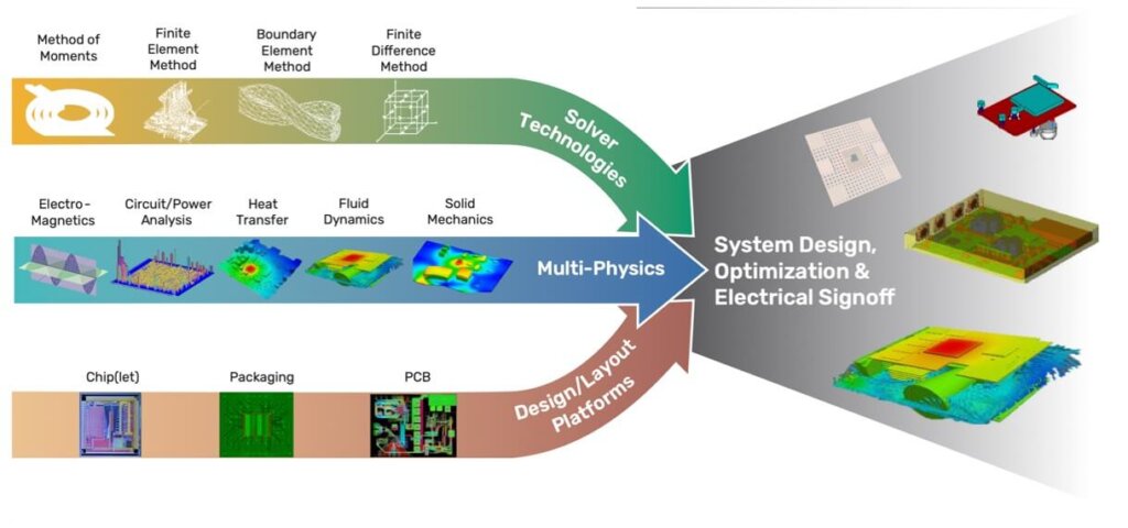
The technical challenges include managing thermal issues in such dense assemblies; ensuring the physical integrity and electrical performance of all the interconnect; dealing with the dramatic growth in the design space that a shift to using chiplets implies; verifying the resulting design in multiple ways; debugging, failure analysis, and more.
One of the key organizational challenges is to manage the way that the use of chiplets blurs the line between IC design and PCB and package design. Each discipline will have to learn more about what the other does, and systems designers will have to understand it all, with access to tools and design flows that bring together aspects of interconnect, IC, and systems design strategies in a tractable way.
Other challenges arise for traditional package designers, including making the transition from understanding laminate-to-silicon-substrate layout and taking on the physical verification process required for silicon interposer designs. There are also electrical and thermal analysis challenges that must be addressed with tools that support in-design and electrothermal signoff, for on-chip and off-chip devices and interconnect.
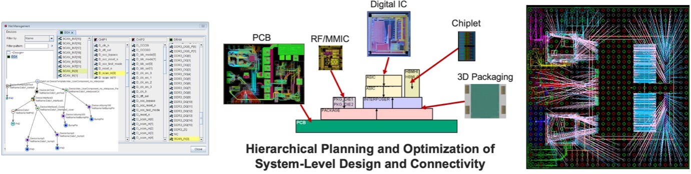
IC designers making the move from monolithic devices to multi-chiplet architectures will have to learn how to plan, manage, and optimize their top-level design and connectivity. This will demand a new breed of tool that can aggregate data from the IC, package, and board design to enable system-level optimization and the development of the top-level netlist necessary for verifying correct connectivity (Figure 3).

The business challenges of establishing a chiplet-based ecosystem may be as complex as the technical ones. When companies make monolithic SoCs, they rely on established test strategies, carried out in-house or by a partner, to ensure their products are working correctly. When their products become complex assemblies of chiplets from multiple vendors, assembled on an interposer made by another company and packaged by a third, the responsibility for final product testing, correct functionality, and overall yield becomes unclear. Many of these issues have been addressed in the development of MCMs, but the solutions, such as the use of known good die (KGD), will have to be retooled for the new level of complexity implied in 3D SIP designs.
Interconnect will obviously be an important enabler for a chiplet-based ecosystem. Companies such as Cadence already have design IP for many forms of on-chip and off-chip interfaces, which customers can instantiate as standard I/O chiplets for use on multiple 3D-IC designs. This will enable them to match their manufacturing process choices to the needs of the I/O standard—for example, to enable them to instantiate electro-optical interfaces.
This design reuse proposition should appeal to large OEMs that can find such common functionality in their product roadmaps. What would make the chiplet ecosystem even more attractive is if such chiplets could be shared outside of a single company, thanks to a common interface standard.
The Universal Chiplet Interconnect Express (UCIe™) standard is being developed to serve exactly this purpose, defining physical interface characteristics such as trace widths, bump pitch and channel reach, and electrical characteristics such as data rates and formats, latency, bandwidth, and testing and compliance issues.
If UCIe takes off, it should make leading-edge functionality available to designers who need to build highly integrated 3D-ICs but cannot make an economic case for monolithic integration on leading-edge processes. Chiplet-based design, though, still needs the support of tools that take a holistic view of the process, and IP that standardizes interconnects. Testing and debugging methodologies must also be improved to deal efficiently with multi-die scenarios.
If all this can come together, end customers can look forward to a continuation of the functional integration trend that Gordon Moore set the industry upon all those years ago.
Editor’s Note: This article first appeared in the 2023 3D InCites Yearbook. Read the issue here.