
For the 8th year in a row, I did NOT attend SEMICON Singapore. But apparently this is the year I should have been there to cover the 3D IC Forum, as it was well attended and had a robust program with 15 speakers and a panel discussion (at least that’s what IME’s Surya Bhattacharya said in a Skype interview.) Luckily many of my industry contacts did attend (and participate) and were more than willing to brief me on the take-aways they found to be most critical. To them I am most grateful.
Bhattacharya, who is Director of Industry Development for the Through Silicon Interposer Program at the Institute of Microelectronics (IME), organized the second half of the afternoon session on behalf of A*STAR IME. Sesh Ramaswami, Managing Director, TSV and Advanced Packaging, Applied Materials, Inc. (AMAT) organized the morning. The event was co-sponsored by IME and AMAT, along with SEMI.
Highlights of the day included a keynote by Toshiyuki Hiroi, Senior VP, Sony Computer Entertainment Inc., who talked about 3D chip stacking for gaming and other consumer applications; a keynote by Mr. Lee Choon Heung, Senior VP, Amkor Technology, who discussed process integration and challenges in 2.5D and 3D TSV assembly; and a 3D panel discussion, 2.5D and 3D: On the Way To HVM moderated by Jan Vardaman, President, TechSearch International.
Cost, Cost, and oh yes, COST
Across the board, everyone agrees that cost continues to be the main roadblock pushing the adoption date further out. Now, for HVM in consumer products, we’re looking at 2016-2017 (2015-2016 for 2.5D mobile application processor on Memory). Vardaman told me these were the dates presented by Hueng, of Amkor. But he’s not alone in this thinking. “Everyone was saying, ‘how do we lower the cost of these so that people can start using this technology?” Vardaman said. She added that researchers from IME commented that Cu back-end-of-line (BEOL) processes are the biggest cost. From the end-user perspective, she said that according to Hiroi, Sony Entertainment currently uses a chip-on-chip technology, and needs a solution that can fit into a price point for boxes that sell between $99 and $299. She said there were discussions on how to improve throughput and temporary bonding/debonding technologies. (You know the drill).
Bhattacharya agreed with Vardaman. “Reduce cost – nothing is more important than that. When the industry talks, we have to listen,” he said. How low does the cost need to be? It probably needs to be less than 1-2cents/mm2 for high volume applications.
In response to the call for lower cost, he said IME has organized a collaborative effort with industry partners to find a solution for manufacturing low-cost interposers. “The mobile space has so many product possibilities. But to address this technology we have to collaborate. One manufacturing partner may not be able to do all things themselves. It’s complicated,” explained Bhattacharya. He added that IME has invested in 300mm BEOL facility in collaboration with Applied Materials that was inaugurated in 2012. It is a full TSV interposer line that includes TSV fabrication, backside processing and a 300mm assembly and packaging facility. The facility is staffed by electrical teams charged with finding solutions to interposer design issues such as signal and power integrity issues and are designing lattices for power distribution. There’s been so much interest in the project worldwide that IME has launched a multi-project wafer (MPW) platform. The model is flexible; research partners can either work with IME for interposer fabrication and assembly/packaging, or ship the interposers to their assembly partners. They’ve even developed a process design kit (PDK) with design rules for fabless companies.
Magic Wand Wish
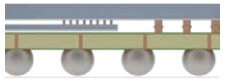
I also spoke with David Butler, VP of Marketing SPTS, to get his perspective as a panelist on the 3D Panel. He said every one was asked particular questions, one of which was, if you could wave a magic wand and solve one issue, which would it be? His wish was for solutions to total thickness variation (TTV) of the Si/glass paired substrates used at the backside processing stage. Butler explained that TTV variations comes from a number of factors including the tolerance of the glass carrier, the flatness of spin-coated adhesives used for temporary bonding/debonding, and the depth non-uniformity of the embedded vias. One of the process steps SPTS’s plasma etch tool performs is via reveal, etching back the silicon on the backside of the wafer to reveal the TSV copper interconnects. “SPTS’s tools are calibrated for precision etching,” said Butler, “However, planarity is also affected by what you’re starting with – in this case the bonded wafer pair. While SPTS’s Omega etch systems can cope with simple modes of non-uniformity, for example, convex or concave. It’s tough to cope with more complex shapes.” In other words, the tool’s effectiveness is only as good as the wafer being processed.
TSV Alternatives
Other than the cost conversation, other topics touched on were alternatives to TSV technologies, and development in silicon photonics.
On behalf of Altera’s John Xie, Vardaman presented slides on a face-to-face copper interconnect technology that doesn’t require TSVs. I spoke to Xie at length about this work, the goal of which is producing low-cost high-density alternatives to TSVs. (Xie recently co-authored a feature with Amkor’s Debra Patterson, published here in Chip Scale Review’s May/June issue.)
Xie explained in this packaging approach, two die are joined face-to-face using Cu micropillar microbumps to form a close connection between the active circuitry without TSVs. He said the unique advantage of this technology is the increased density for a 2.5D interposer, which allows for further parasitic reduction, latency and power reduction. There are no limitations on the number of die that can be accommodated; however its critical that one die is sufficiently larger than the other in a mother/daughter configuration to avoid a bottleneck.

Xie said this technology targets FPGA technology for telecom, computing and data applications. Primarily a large die configuration, Xie says fundamentally, the concepts of the technology could be applied to mobile devices. One point he wanted to make is that “high density does not mean high cost, low density doesn’t mean low cost.” He added that there are more and more low-cost alternatives being offered, citing the MEPTEC conference last spring that featured a number of low-cost alternatives including high density organics.
On the topic of organic interposers, Bhattacharya says while it has promise in certain application spaces, it has its pitch challenge and overall still thinks silicon as an interposer material is the way to go.

Silicon Photonics
Silicon Photonics keeps popping up at 2.5D and 3D IC technology conferences. Bhattacharya says that’s because it’s becoming critical to bring optical communications closer to the electronics, and that silicon photonics can do that. IME is beginning to explore integrating photonics into the interposer side by side with the logic die. The value-add of Si Photonics, particularly in data center applications, where investment in technology can reduce overall costs by reducing power consumed. As such, IME sees a future for both passive interposer technology and active interposers with photonics, and is pursuing both areas.
Featured photo: through silicon stack (TSS), courtesy A*STAR IME’s Facebook page


Great observations, especially that about cost moving things to the right..
Its good to see that some of the marketing derived fog is finally clearing up from 3-d stacking activities and consensus developing among the stakeholders / potential users based on hard Physics & Economics.
However the over – hyping of 3-d stacks w/ TSVs seems to have now shifted to 2.5 -d as the new savior ( simpler process & heat removal ). To justify the switch from organic substrate based modules to more expensive Si interposer based 2.5 – d modules it is necessary to examine their clear advantages ( tight integration of chips with dissimilar technologies, improved electrical performance – both derived from higher interconnect density ).
The much higher interconnect density possible when current Organic substrates are replaced by Si substrate w/ finer geometries ( e,g. L/S of 1 or 2 um and Via Pitch of 30 um, micro – pillar FC bumps ) enable superior electrical design for power delivery, differential lines / signal integrity etc. But in spite of these electrical advantages derived from higher interconnect density the length of ea. interconnect between 2 adjacent chips in a fine – pitch Si Interposer based 2.5–d module, would still be not much shorter than the sum of half – lengths of those 2 chips – a dimension far closer to that in an Organic substrate rather than in a true 3-d stack w/ TSVs. So the Bandwidth / Power improvement in a 2.5 – d would hardly be as impressive as in a 3D-TSV.
Much anticipated high volume applications of 2.5 – d modules e,g. GPU / memory would require dice far smaller than 40 mm sq. behemoths ( FPGAs before Xilinx built their 2.5 – d module ) and so would not benefit from the Fab yield related cost savings of partitioning a large die. As to CPU – memory – I/O modules even for Servers, given near term Memory roadmaps, most would not be able to take advantage of the increased interconnect density afforded by a 2.5 d interposer.
Given such marginal improvement / window for Si Interposer 2.5 – d modules over even current Organic modules, one would expect that only for very critical applications ( Defense, Medical,.. ) would it be possible to justify the additional cost of this reincarnation of ’90s era MCM – Ds.
The TSV – less “Possum” alternative promoted by an OSAT looks quite similar to Inverse Flip Chip based MCM – Ds developed at Motorola SPS ( US Patents No. 5,198,163, ..). It is a promising configuration so long as the I/O of individual daughter chips line up with corresponding I/O on the large mother chip. Otherwise redistribution would become necessary, imposing not just cost but performance penalties.
Good summary Francoise!
There is universal agreement that the costs of TSV-based interposers need to come down radically for 3D IC stacking to become commercially viable. To that end, what is needed is faster & cheaper via plating alternatives and compliant & thermally conductive substrates to address thermal and thermomechanical challenges.
MP Divakar