
The monthly MEPTEC Luncheons at SEMI in Milpitas focus on microelectronics packaging and test topics. Javier DeLaCruz, Xperi’s VP of Engineering, presented at the latest Luncheon on January 8 a joint study with eSilicon. It compared how die-to-wafer (D2W) bonding, using Direct Bonding Interconnect (DBI) technology, compares with traditional (2.5/3D-IC) assembly approaches for multi-die integration into a package.
Multi-die Integration
Decreasing feature sizes of transistors and on-die interconnects improve performance per Watt for integrated circuits (ICs) and systems. However, the maximum reticle size of 33×26 mm (~ 856 mm2), the rapidly decreasing yield achievable with larger dice, and the resulting increase in unit cost limit the complexity of cost-effective single-die integrations. Multi-die integration of ICs (2.5/3D ICs) is coming to the rescue. It can make high levels of homogeneous as well as heterogeneous integration cost-effective and expand significantly how much functionality an IC package – or module – can contain. Vertically stacked dice (in 3D ICs) promised initially to make interconnecting multiple dice with through-silicon vias (TSVs) very easy, however, cooling challenges, limited EDA tool capabilities, and the need to closely coordinate designing of all dice in a stack, are major factors to limit 3D IC market acceptance.
Arranging dice side-by-side on an interposer (2.5D integration) or directly on a substrate simplifies heat management but enables high-speed interconnects only to adjacent dice. In addition, traditional dice to interposer/substrate connections use relatively large micro-balls or copper-studs and with them introduce significant RC delays and extra power consumption for charging/discharging these interconnects. DeLaCruz’s presentation demonstrated that Xperi has been addressing and solving several of these multi-die challenges.
DBI Ultra to The Rescue
As the alignment accuracy of die-to-wafer bonders is continuously improving – currently at 3µm, projected to decrease to 1µm –DBI Ultra developed by Xperi, becomes attractive for improving performance while reducing power dissipation and unit cost.
Xperi and eSilicon used a 51.2 Tbps switch application to compare a DBI Ultra-based design with traditional multi-die assembly techniques – see Figure 1.
More about Multi-Die Integration Options:
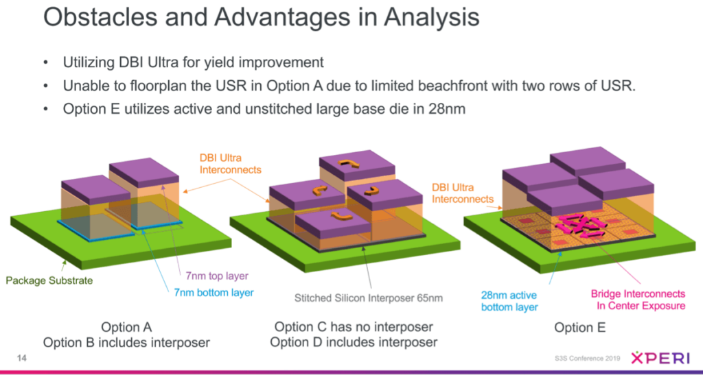
- Option A uses ultra-short-range (USR) SERDES to interconnect the needed circuits, implemented on TWO dice and mounted directly on a substrate.
- Option B uses high-bandwidth interconnects (HBI) to connect the TWO dice on an interposer that’s mounted on a substrate.
- Option C uses USR SERDES to interconnect the needed circuits, now implemented in FOUR dice, only with their ADJACENT dice, directly on a substrate.
- Option D uses HBIs to connect the FOUR dice on a 65nm passive interposer, only with their ADJACENT dice.
- Option E uses HBIs to connect FOUR dice, mounted on NINE 28 nm bridge dice, each with an active area in the middle, to enable direct high-speed interconnects between ADJACENT dice and ALL FOUR dice in the center of this assembly.
Placing four dice onto nine bridge circuits and using DBI Ultra technology, provided clear unit cost, power, and latency benefits. However, the needed bridge dice increased tooling cost, compared to options A to D (Figure 2).

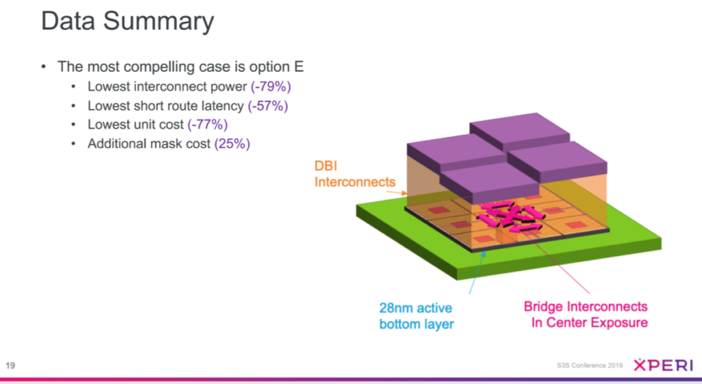
Figure 2: Summary of power, latency and unit cost benefits; also considering the increased tooling cost. Courtesy: Xperi
Conclusion
Narrower scope centered around continued feature size shrinking: Moore’s Law originated at Intel and has been applied very successfully for integrating more and more functionality on a single die. It has served our industry well for more than 50 years, but the above-mentioned challenges triggered taking a closer look at it.
Moore’s “Law” is not really a law, but an observation made as integration density on single dice ICs increased rapidly during the 1960s and beyond. The increasing need for heterogeneous integration, market demand for entire (sub)systems in a single package, the exploding development cost and time to profit for very large single-die ICs and other factors encouraged our industry to not only apply the traditional “Moore’s Law Thinking” to IC and system design but view multi-die ICs and modules as natural extension of Moore’s original observation and as viable paths to system-level integration. Even Intel no longer relies only on shrinking feature sizes. They developed Embedded Interconnect Bridge (EMIB) technology for 2D multi-die interconnects, Foveros for 3D interconnects and applied both in their recently introduced Lakefield processor.
Broader scope, considering the ongoing convergence of Internet of Things (IoT), 5G wireless and artificial intelligence (AI): As more sensing, computing and data transmitting capabilities must be moved to the edge of IoT networks, cost-effective, small and ultra-low power integration of heterogeneous functions is becoming even more important. The above discussed DBI Ultra technology, other multi-die interconnect and assembly technologies (like wafer/panel-level packaging, flexible hybrid electronics and others) as well as optical communication links will become important differentiators for highly integrated, multi-physics sensor nodes, pre-processors and multi-standard communication links. Only a well-coordinated supply chain – from system planning tools all the way to manufacturing flows and equipment for high-volume assembly and test – will meet these challenges timely and cost-effectively and continue (hopefully accelerate) revenues and profit growth for our industry.
Health, Prosperity, and Success in 2020 and beyond! Thanks for reading…Herb


