
Samsung reports that they have seen increasing interest in multi-die integration (what they call MDI) for markets such as artificial intelligence (AI) and high-performance computing (HPC). They also report a need for new electronic design automation (EDA) solutions because the traditional design doesn’t fully address the latest power and signal noise challenges.
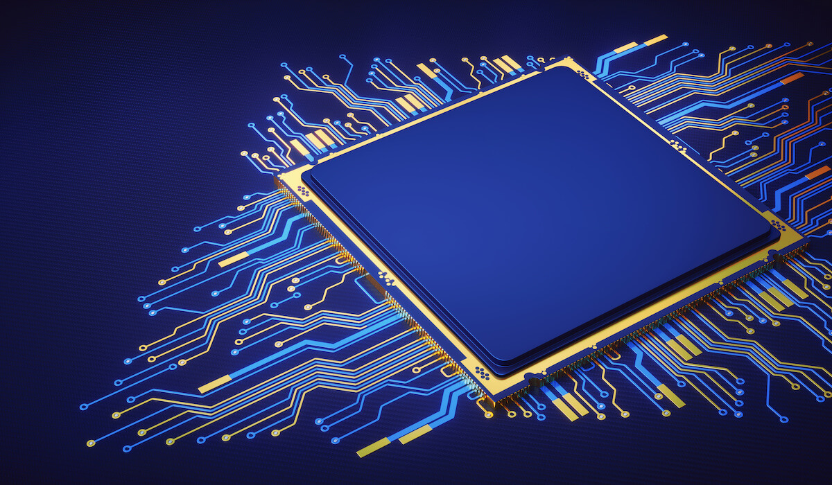
Advanced packaging technologies simplify production and increase the performance of highly complex multi-die systems-on-chip (SoCs) as the semiconductor industry is looking at chiplet approaches as an alternative to large dies that take a longer time long to develop and are expensive to make. Samsung Foundry offers customers a 2.5D-IC Multi-Die Integration (MDI) design flow that incorporates analysis and implementation for early-stage system-level pathfinding to help overcome potential issues (Figure 1).

In related news, the company has recently qualified Synopsys and Cadence design flow support software to simplify the overall design development process.
Samsung Foundry currently offers 2.5D-IC MDI flow for chips produced using its 7LPP (7 nm with several EUV layers) fabrication process and its SUB20LPIN silicon interposer. According to the company, “Samsung Foundry’s MDI design flow, which integrates analysis and implementation for early-stage system-level pathfinding, enables customers to overcome performance issues and achieve cost-efficient 2.5D-IC products. i.e. “Coupling noise between multi-die and package causes unexpected performance issues, and addressing 2.5D-IC system problems at later design stages is more difficult as design complexity increases.”
Synopsys Jumps on Board the Multi-die Integration Train
Samsung’s 2.5D-IC MDI flow is now supported by Synopsys’ Fusion Design Platform and Custom Design Platform software packages that are used to develop SoCs.
The Synopsys EDA tools allow for automated silicon interposer creation and routing; routing among micro-bumps, TSVs, and C4 bumps; power network design; EM/IR analysis of multi-dies and interposer; automated SPICE deck generation for power; and signal integrity analysis of HBM and high-speed interfaces. Functionality of their software suites is described in the table below.
By launching its 2.5D-IC MDI flow for 7LPP technology and SUB20LPIN silicon interposer, Samsung Foundry reportedly aims to simplify the development process for its customers who adopt a multi-die/chiplet approach for their devices aimed at high-performance computing, AI, and other performance-demanding applications (Table 1).

Cadence Tools Qualify for Multi-die Integration
Cadence has also announced that its 3D-IC advanced packaging integration flow has also been certified by Samsung Foundry for its 7LPP MDI (Multi-Die-Integration) packaging flow. More information on the Cadence tools that support the Samsung Foundry MDI packaging technology is available here.
The Cadence technology provides customers with analysis, implementation and physical verification capabilities and offers early-stage system-level pathfinding and highly complex design capabilities for 3D signoff.

Cadence’s MDI flow, supports the integration of multiple application-specific die and chiplets into a single packaged device. A full suite of Cadence digital and signoff, as well as IC package and PCB analysis tools, have been optimized for the Samsung MDI technology to guarantee seamless integration for handling multiple dies including the Innovus™ Implementation System, Quantus™ Extraction Solution, Tempus™ Timing Signoff Solution, Voltus™ IC Power Integrity Solution, OrbitIO™ interconnect designer, SiP Layout, Sigrity™ XtractIM™ technology, Sigrity XcitePI™ technology, Sigrity SystemSI™ technology, and Sigrity PowerDC™ technology.
The Cadence 3D-IC packaging flow provides a fast path to design closure and supports the company’s overall Intelligent System Design™ strategy, enabling advanced-node system-on-chip (SoC) design excellence.
DoD Awards BRIDGE $20MM Contract
BRIDG, a Florida based, not-for-profit, public-private-partnership, operates an advanced microelectronics fabrication facility enabling state-of-the-art “manufacturing” for industry and government.
The U.S. Department of Defense’s Industrial Base Analysis and Sustainment (IBAS) office has just awarded BRIDG its first major federal defense contract valued at up to more than $20 million to provide a new technology for “next-generation microelectronic multi-chip systems that will strengthen national security and cyber resiliency for the United States defense industrial base”. The IBAS program is dedicated to strengthening the defense industrial base. The most pressing defense industrial base issue is reportedly the ability to make secure microelectronics in the United States.
It sounds a bit like this is aligned with the recent SHIP contracts we detailed in IFTLE 422 and 429.
“The microelectronics that are used in large defense projects are frequently outsourced or made by foreign-owned companies. Securing the microelectronics supply chain is a priority of the Department of Defense and this award is the first step in a larger effort that the federal government is beginning to undertake.”
For all the latest in Advanced packaging stay linked to IFTLE……………………………


