
At ECTC 2013, Dow Corning Corporation (DCC) introduced its solution to the temporary bond/debond conundrum. During the materials and process session, Ranjith John, materials development & integration engineer at Dow Corning, presented a paper titled Low Cost, Room Temperature Debondable Spin on Temporary Bonding Solution: A Key Enabler for 2.5D/3D IC Packaging, co-authored with equipment supplier, SÜSS MicroTec. In his presentation, John, explains the development of a bi-layer spin-on temporary bonding material that doesn’t require special equipment for the pre or post treatment steps. The result is increased throughput which translates to lower cost of ownership. I caught up with John and with SUSS’s Wilfried Bair to find out the details and impact this introduction will have on meeting the temporary bond/debond challenge.
So what differentiates this solution from all the others that claim to solve the challenges of temporary bond/debond steps? John explained that while others say they are a room-temperature debond process, they all have to do something – laser treatment, chemical solvent, a heated chuck – to initiate the debond. Additionally, typical temporary bond processes require heating the bond chamber enough to liquefy the adhesive and then cooling it to set. This means lots of time in the bond chamber.
According to John, Dow Corning’s solution doesn’t use heating during the bond step or the debond step. The entire process takes place at room temperature. “We don’t have to do plasma pretreatment, or laser or chemical post treatment. This translates to lower cost of ownership (CoO) for the temporary bond/debond process,” said John. The “magic material” is based on Dow Corning’s proprietary material chemistry and has demonstrated both chemical and thermal stability.
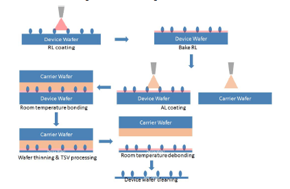
So how does it work? John outlined what he called a “simple bilayer solution” involving spin coat of a thin release layer on the active wafer followed by a spin coat of thick adhesive material. Then the carrier is bonded to the active wafer, however, John points out, the bond is formed between the release layer and the adhesive rather than to the wafer. The only step that does require heat is the cure step, which happens outside the bond chamber on a hot plate (Figure 1).
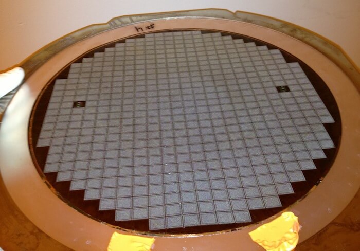
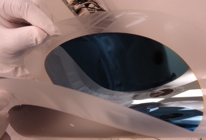
Once the backside processing has taken place, the debond step is a mechanically initiated peel/lift off step. As previously mentioned, the debond happens at the release/adhesive interface. The device wafer then goes through a final spray clean step to remove any remaining residue, and voila! – successful crack-free debonding (Figure 2). The entire process takes only a few minutes to complete. It’s important to note that this whole sequence has also been successfully demonstrated on bumped wafers.
As I’ve been following the temporary bond/debond story for some time, I was curious to find out SUSS’s involvement in all of this. Thus far, the tool supplier has qualified a number of materials and processes on their temporary bond/debond equipment. DCC’s process joins the ranks of Dupont, 3M, TMAT, Brewer Science, and Dow Electronic Materials. According to Bair, SUSS collaborates with all these material vendors in order to keep its equipment material agnostic.

From Bair’s perspective, its important to demonstrate that SUSS’s bonding tools are compatible with any material and process available on the market. This is because there are a number of applications within the 2.5D and 3D IC realm, as well as other markets (MEMS and compound semiconductors, for example) that respond well to different bond and debond steps. To be married to only one material and process would limit SUSS’s flexibility.
Throughout working with all the different vendors, Bair said he sees the advantages and disadvantages of the different temporary bond/debond processes and materials that are available in the market today. What’s important he says, is matching the right solution to the right application to maximize benefits and minimize the risks. In that case, the more options the better.
In the case of Dow Corning’s solution – the aim was to develop a low cost solution with increased throughput for high volume manufacturing (HVM). Development work strongly indicates that this is the case so far. 3D InCites will follow the progress as it unfolds.


