
It’s too bad SUSS MicroTec’s Wilfried Bair was one of the last presenters on Friday at 3D Architecures for Systems in Packaging Symposium (3DASIP), Dec. 14, 2012, because more people should have been present to hear what he had to say. While most presenters focused on successes and future work for optimization and lower cost of ownership, he really went out on a limb to explain why there are such divergent reports on temporary bond/debond (TB/DB) readiness, and painted a more realistic picture of the actual situation.
Bair remarked how many of the papers we had heard throughout the past few days indicate that the industry is ready, but that TB/DB that are not ready for manufacturing for 3D TSVs. “On paper it works, on PowerPoint it works, why do users disagree?” he asked, and then went on to answer his own questions. “ There’s a gap in what gets reported and presented, and what actually happens in the manufacturing environment. The gory detail don’t get shared,” He said, and then proceeded to share them. The reality is that process areas and target results are largely affected by challenges in:
- Voids
- Total thickness variation (TTV)
- Coating of high viscosity adhesives
- Adhesive Conformity to topography
- Adhesive strength varying with topography
- Mechanical stability of adhesives for backside processing (grinding)
- Thermal stability
- Particles
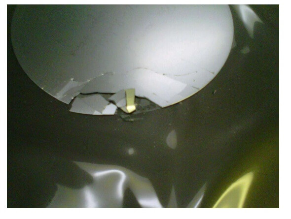
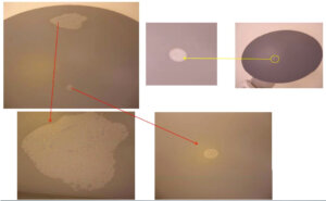
As we all know, pictures speak louder than words, and Bair shared the following examples of voids, what happens when adhesives are too strong, and lastly what happens when adhesives are too soft.


Collaboration between equipment and materials providers need to focus on finding the ideal combination of compliance and rigidity to make it happen. However, Bair says specifications and requirements are “a moving target”. For example, the carrier material, silicon or glass, affects the adhesive material changes. “Every adhesive manufacturer does its own testing before we even start testing,” he said. “In the end, a combination of factors is needed before we can really verify all the backside process. There is a difference between running dummy wafers and actual device wafers.“
Bair highlighted specific technology solutions that need to be worked on over the next six months as follows:
- TTV: 49 points no exclusion zone
- Squeeze out: Adhesive that extends beyond the end of the wafer bevel. With and without edge trimming.
- Thinning: Grind and polish to 60µm; look for wafer breakage, edge chipping, delamination and good TTV.
- Thermal-250C 250C for 30 min: In air, look for dimples on a thinned wafer. Measure for 30 min: In air, look for dimples on a thinned wafer. Measure voids/delamination.
- Thermal-400C slow ramp: In Nitrogen atmosphere. Goal is to have a 5 min test. Currently using a box oven, so slow ramp. Look for degradation of the adhesive.
- Vacuum: 10 -4Torr, outgas measured with an RGA. Should not see any outgas
- CMP: Look for wafer breakage, edge chipping and delamination. Good TTV. No chemical reaction to Al2O3 and SiO2slurries.
- Solvent: Solvent: Tested with eleven chemicals (details next slide) Tested with eleven chemicals (details next slide)
- De-bond: Room temperature mechanical de-bond without damage to thinned wafer. No visible residue using 50X optical microscope.
- Carrier clean: Mechanical clean or SRD clean or wet bench clean.
Additionally, Bair noted that over the next 12 months, business solutions to be worked out include per wafer cost; throughput; footprint for bond, debond, and clean; identified yield factors and maximize yield. He cited specs and requirements as “the moving targets”.

“The process has to be there, the technology solution has to be there, before we can tackle cost-of-ownership (CoO) and reduced cost,” noted Bair. Once the technical requirements are met, the cost is too high for volume production, but volume production is needed to decrease cost. And therein lies the chicken-and-egg conundrum.
But on the bright side, all of this spells opportunity for materials manufacturers who are charged with coming up with the solutions. And at some point, come hell or highwater, 3D ICs will happen. ~ F.v.T.


