
Of all the companies that have supported 3DInCites over the past 10 years, none has been more consistently involved, both as contributor and sponsor, as EV Group. In fact, without EVG’s belief in our mission and their sponsorship the first three years, I doubt 3DInCites would still exist today. Therefore, it seemed fitting to honor them with the cover story for our 10th Anniversary print edition; The First Decade.
Since the beginning of 3D integration, EV Group has been there. They were the first to invest in R&D for image sensors. They implemented the first fusion bond and the first layer transfer for sequential 3D stacking. The inventors of temporary bond/debond (TB/DB) processes, their solutions are as old as the market, back when they were referred to as tape mounting systems, notes Paul Lindner, executive technology director at EV Group.
“We are a technology provider,” he said, “The equipment industry has to be. There are no high-performance chips without the right tools.” Additionally, he said, it takes a combination of processes, materials, and equipment to achieve success. The burden of optimizing those processes falls to the tools. “Equipment has to continually improve and optimize,” said Lindner.
Visits to EV Group Headquarters
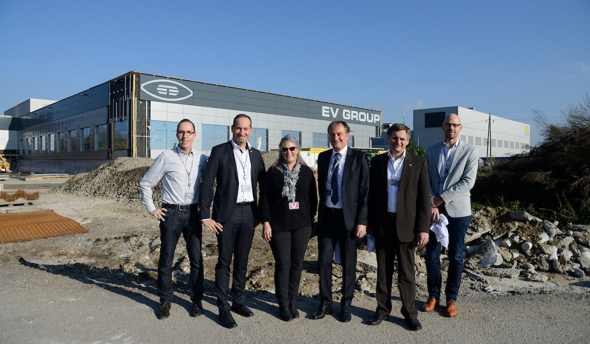
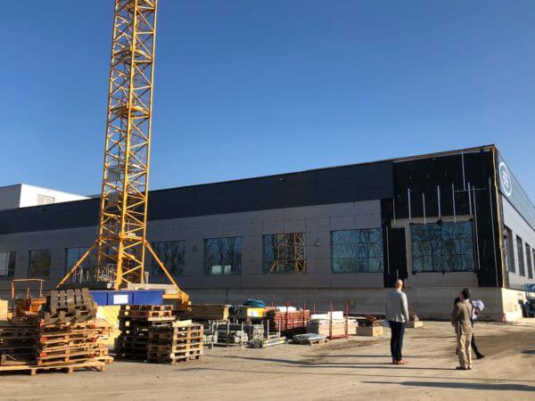
In the past 10 years, EVG has grown exponentially. I have been invited to tour the ongoing expansion at corporate headquarters in Schärding, Austria four times. The first time was in 2010; the year of the company’s 30th anniversary. I returned in February of 2012, January 2014, and most recently in November 2018 (Figure 1)
Since 2009, the manufacturing area grew from about 3,100 to 7,100m2, the machining center from about 1,900 to 3,600m2, and the cleanroom area from about 1,200 to 2,800m2, says Clemens Schütte, director of marketing and communications. In the same period of time, the number of employees worldwide increased from 430 (Sep 30, 2009) to more than 860.
Triple I Today – November 2018
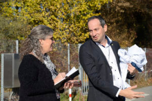
My most recent visit to EVG included a construction site tour and lunch with members of EVG’s leadership team including Werner Thallner, Paul Lindner, Hermann Waltl, and Thomas Uhrmann, as well as Clemens Schütte and Klaus Doblmann from the marcom team (See feature photo above).
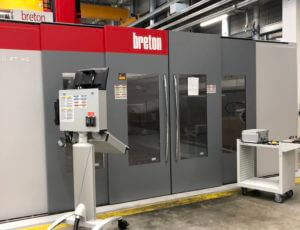
In the four years since I last visited EV Group, a new machine shop and test room building were added. The new machine shop was built around the old one, doubling its size to 3600m2. It features a new CNC milling machine large enough to machine parts that larger tools require for handling a variety of substrate sizes, such as for panel level packaging for fan-out wafer level packaging, or flat panel displays (Figure 2).
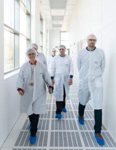
On this particular day in the class-1 clean test room, a next-generation fusion bonding systems (Gemini FB XT) configured for hybrid bonding of image sensors and stacked flash memory was being put through its paces (Figure 3). This tool features cleaning and plasma activation module used for preconditioning wafers before bonding, and the latest SmartView NT3 aligner, its alignment accuracy from 500nm to 50nm: 10X in 10 years.
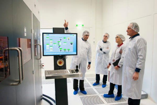
“That’s better than Moore’s Law,” noted Thallner. “While speed and accuracy are both important for 3D and we are working on both, alignment is more critical. Verification of alignment directly after bonding is critical for high yield too. We are the only company that offers alignment verification integrated into the fusion bonder.”
Two robots keep the wafers moving. The floor in the test room is raised so that connections can be made under the floor.
The latest construction, dubbed Manufacturing Building III, will connect manufacturing with final assembly and test so that there is no need for customers to walk outdoors (Figure 4). In addition to expanded manufacturing and warehouse space, there will be a designated packaging area designed specifically for cleanroom equipment. Shipping and receiving will be centralized in a restricted area, as the company is authorized to inspect tools for shipping.
In Growth Mode
These days, the company is fully immersed in all aspects of heterogeneous integration with its tools and processes that support all the elements of bonding and lithography.
More than Moore is on the rise, says Lindner, and the company’s Triple-I approach – Invent, Innovate, Implement – is paying off as all the markets they touch are in growth mode, from advanced fan-out wafer level packaging (FOWLP), interposer and 3D integration, to compound semiconductors and MEMS, photonics, biotech, and flat panel displays.
“It’s been a long journey from the first lithography line for 3D packaging to industry adoption; a lot longer than we expected,” noted Lindner. “And the nano-imprint lithography business took more than 15 years from invent to implement. It’s important to start as early as possible and scale the process. You can’t make a ‘side entry’ into a market when it ramps to high volume and expect to succeed.”
For example, the company has more than 20 years invested in TB/DB R&D and has been through all the technology changes, from thermoplast and mechanical debonding, to zone bond invented together with Brewer Science. The different TB/DB methods suit different applications, and EVG supports them all.
Submicron Accuracy Bonding
EV Group is perhaps best known for its advancements in permanent wafer bonding tools, where it is a market leader. Uhrmann says new application drivers like artificial intelligence and machine learning require high levels of computing at the edge and cloud. This calls for high-density interconnects that are bonded at pitches of 2µm or smaller. As a result, interest is growing for fusion and hybrid bonding processes.

Understanding the growing importance of alignment accuracies for fine-pitch applications, its latest-generation SmartView® face-to-face bonder alignment system features 50nm alignment, as previously mentioned. Armed with the SmartView NT3 system, EVG’s flagship automated fusion bonding system, GEMINI® FB XT, supports applications requiring higher alignment accuracies, such as memory stacking, 3D systems on chip (SoC), backside-illuminated CMOS image sensor (BSI-CIS) stacking, and die partitioning.
The company’s latest tool introduction, the BONDSCALE™ automated fusion bonding system, is designed to support a broad range of fusion/molecular wafer bonding applications, including engineered substrate manufacturing and 3D integration approaches that use layer-transfer processing, such as monolithic 3D (M3D). With this tool, EVG brings wafer bonding to the front end.
In addition to wafer-to-wafer hybrid bonding, EVG is also working in collaboration with imec to develop wafer-to-wafer processes, to be able to increase throughput, in addition to achieving 50nm alignment accuracy.
The Road to 3D TSV Adoption
After lunch, Uhrmann and I sat down to reminisce about the past 10 years, and specifically the longer-than-predicted road to 3D TSV adoption. Beyond the well-known cost challenge, there were other technology issues that delayed progress.
One of the biggest challenges was regulating the keep-out zone around devices to reduce the impact of TSV-induced stress. “Managing the stress in a 3D wafer is not a piece of cake,” noted Uhrmann. Bow and strain caused by how the wafers react to copper called for process adaptations for the whole fab supply chain, from substrate changes to etching and deposition processes to debonding methods.
Did the development of FOLWP slow down progress for 3D TSVs? Uhrmann says no. To the contrary, he says he thinks fan-out technologies put advanced packaging – including 2.5D and 3D TSVs – on the prime stage. It became clear that heterogeneous integration through advanced packaging was the way forward to achieve more functionality and performance.
The semiconductor industry is notoriously slow to adopt new technologies. As long as 2D approaches worked, there was no reason to change, explained Uhrmann. It wasn’t until there was no other way to achieve performance requirements, that 3D TSV was adopted.
Uhrmann credits the smartphone – and particularly the iPhone 3S – for ramping BSI-CIS into volume production. Next came memory stacking, using TSVs in DRAM stacking to achieve high-bandwidth memory (HBM), but that took longer to achieve.
Small devices, such as smartphones, changed the entire industry. And now artificial intelligence that enables cloud and edge computing are driving performance requirements even higher, while also driving down-power requirements.
“This is what is pushing advanced packaging. We need the flexibility that you can’t get with just chip design,” says Uhrmann. “It’s not just about logic anymore, it’s all about systems. Advanced packaging is how you smartly connect dies. 3D will be everywhere for More than Moore technologies.” And when that happens, you can be sure EVG will be ready for it. ~ FvT To read the full cover story and see more photos, download the print issue here.
UPDATE: Check out EV Group’s recent announcement of yet another expansion.


