
We’ve all heard it: Wide I/O DRAM on Logic using TSV interconnects will be THE solution for achieving the high performance/low power needs of next generation devices, beginning with the high performance computing and making its way into gaming processors, smartphones and tablets. To listen to the experts, meeting such performance goals as true HD, faster video streaming, multi-cameras, multi-application operation, and other processor-intense applications that require higher bandwidth at slower clock speeds can only be done with Wide I/O (Figure 1). Unfortunately, it looks like manufacturing logistics will push out the previously scheduled forecasted timeframe for Wide I/O DRAM on Logic package configurations from 2014 to as late as 2016. So what are we to do in the meantime?
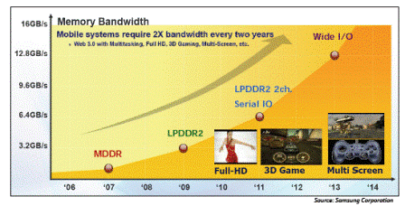
Figure 1: Roadmap of memory bandwidth requirements (Source: Samsung)
Today, Invensas launched a potentially innovative solution to this conundrum: they call it the bond via array package on package (or BVA Pop), which reportedly “delivers performance required by mobile OEMs while preserving the proven infrastructure and business model of traditional package-on-package (PoP).” According to company CEO and president, Simon McElrea, BVA is a technology that can be used “right now” to achieve performance benefits that otherwise will have to wait until 2016 when wide I/O TSV will be ready.
Invensas is a one-year- young, wholly owned subsidiary of Tessera, and has invested $100M on patent acquisitions focused on circuit design, materials, memory modules, 3D architectures and advanced interconnect technologies. BVA PoP is the second product launch (the first was its multi-die face down product family (xFD)) for Invensas, and the first in the 3D packaging space.
How it Works
The technology is an improvement on the traditional PoP thanks to a novel method of interconnect that replaces either solder ball stacking or solder filled laser vias as the method of connecting the top memory package to the bottom logic package. Instead, copper wire bonding processes are used to create free standing pins that are then overmolded for stability, with the ends exposed to create the interconnect to the top package. A dimple in the mold surrounding the exposed pin helps the solder ball from the top package stay in place (Figure 2).

Figure 2: Copper pin formation on the bottom package. The bottom package can accomodate a number of rows, that allows for a higher number of interconnects.
The result is a PoP configuration that is 0.300.2mm pitch with 432-1512 interconnects vs. 0.65-0.5mm pitch and 168 interconnects of a traditional solder ball stacked PoP or the 0.5-0.4mm pitch and 240 interonnects achievable in a solder flled via PoP (based on a 14x14mm package) (Figure 3).
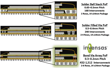
FIgure 3: Comparison of BVA with traditional solder ball stacked POP and Solder Filled Via Stack.

Only the bottom package goes through the pin process. The top package is a standard memory package. One of the beauties of this technology, according to McElrea, is that it uses standard equipment with custom tooling (kit available) for wire bonder and overmold equipment.
Only a Bridge Technology?
Using current technologies, when bandwidth is increased, so are clock speeds. This puts a strain on the battery, draining it in half the time. Moving to Wide I/O allows for higher bandwidth without increasing clock speed. However, it requires 3D ICs to be ready. The trick of BVA, explained McElrea, is that you can achieve the same number of I/Os but don’t have to use TSV achieve it. “If you can do 1250 interconnects,” explains McElrea, “You can run the clock 4 times slower and get the same bandwidth as with Wide I/O using TSV.” However at some point, he admits, BVA will not reach the same power levels or provide the bandwidth required on the TSV roadmap. But it’s a great way to use the existing infrastructure to achieve ultra-high I/Os for improved performance today. He also believes that BVA has more longevity than as a bridge technology. “In packaging, nothing ever dies, it just becomes a new standard, “ he noted. “TSV will address super high functionality devices, but you can build every cell phone on everyone’s roadmap for years with BVA. Eventually, TSV will be the only way to do it.” In this way, BVA is more than just a bridge, but will coincide nicely along with Wide I/O DRAM on Logic when it is commercialized. And rather than pushing out Wide I/O TSV further, as was implied in the press release, BVA is providing a viable solution until Wide I/O appears on the scene, and will also fill a need for a high performing, low-cost alternative once it does.
Interested in learning more?
Invensas will present its BVA PoP solution at the Electronic Components and Technology Conference (ECTC) at the Sheraton San Diego Hotel and Marina in San Diego. Titled “Fine Pitch Copper PoP for Mobile Applications” the paper will be part of Session 31, “Applications With 3D Technology,” at 4:45 PM on Friday, June 1, 2012. Invensas will also exhibit at ECTC in booth 107 on May 30 and 31, 2012.


clever.
any risk of shorts / non – wets when the solder bumps at 0.2 mm pitch on the top package are ” flip – chip ” bonded to the bare (?) Cu-wire “posts” sticking out of the bottom package
any electrical measurements ( e,g. bandwidth ) yet ?