


In the last 40 years, the Principality of Liechtenstein has evolved from a purely agricultural state into one of the most highly industrialized countries in the world. But some how it has managed to keep its Alpine charm. That’s why at first glance, the city of Balzers, complete with its hilltop castle, did not strike me as a place to find a major manufacturer of high tech semiconductor equipment. But it’s been home to Oerlikon Systems since its original incarnation as Balzers Coatings since 1946. This was my last stop on the Europe in 3D part 2 Tour, and it was a lovely way to wrap-up to 2 busy weeks.
The Oerlikon Group itself is a large corporation, employing 12,700 people structured into five segments including Advanced Technologies (Oerlikon Systems); the Segment Coating for industrial coating of components and automotive parts (Oerlikon Balzers); the Segment Vacuum (Oerlikon Leybold Vacuum); the Segment Drive Systems (Oerlikon Fairfield and Oerlikon Graziano) and the Segment Manmade Fibers (Oerlikon Barmag and Oerlikon Neumag). The purpose of my visit to Oerlikon was to learn more about its activities in the semiconductor field, and in particular, its position on 3D integration technologies as the industry prepares for 3D IC high volume manufacturing (HVM). Albert Koller, Head of Semiconductors at Oerlikon Systems was my host for the visit, and we were joined by Robert Mamazza, CTO of Oerlikon Systems; Jürgen Weichart, Senior Scientist in R&D; and Antonio Calvosa, Head of Business Development.
The core competency of Oerlikon Systems is physical vapor deposition (PVD) thin film sputtering, and the two main markets it serves with its tools are semiconductors (and related markets) and touch panel manufacturing. Koller explained that on the semiconductor side, the two biggest market applications are wafer level packaging (WLP) and power semiconductors. Calvosa shared market data that indicates Oerlikon is a market leader in PVD tools for WLP, and that the four leading OSATS (ASE, Amkor, SPIL and STATS ChipPAC) use Oerlikon Systems.
The company has developed three unique system platforms to handle the different market needs. I saw each of these tools on their facility tour. We first had a window tour of the R&D clean assembly lab, where wafers are run to test the tools, and a metrology lab is used to measure thin films. Next we went into the tool assembly area, where Mamazza identified each tool and explained the details.
The SOLARIS, which was developed for antireflective and contact material deposition for photovoltaic cells, has also found purpose in the manufacture of touch panel displays for smaller form factors, as well as thermoelectric generators for power conversion. The benefits of this tool lies in its throughput capabilities. Mamazza explained that the wafers and panels go through the system’s modules in a serial process they call “indexing”, rather than a batch, and can accommodate throughputs in excess of 900/WPH. The SOLARIS S380, designed for larger substrates than the standard SOLARIS, was being assembled to perform fundamental processes and hardware development for touch sensor technologies. “If we have to modify the hardware, that happens here,” he explained.
Next we saw the CLUSTERLINE® 200 in the R&D lab, which is highly configurable for different processes and device types. It is a PVD sputtering tool handling wafer formats up to 200mm for a number of semiconductor and related markets such as advanced packaging, power semiconductors, MEMS, LED, and compound semiconductors. Flexibility is often as important as throughput, noted Koller, many MEMS and compound semiconductor manufacturers don’t need high-volume tools for single applications.
“CLUSTERLINE® tools are providing the flexibility we need for the different applications we serve,” noted Koller. “This tool handles different process steps of a large variety of applications,”
“It is also ideal for the R&D lab since processes developed can be directly used in the production,” explained Mamazza. This is the same type of tool I saw in action during my visit at Fraunhofer EMFT in January.
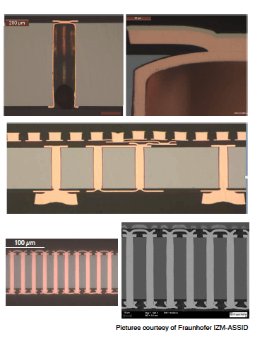
The CLUSTERLINE® 300 handles 300mm wafers, and is targeted to the same process class. There is one of these in the lab at Fraunhofer IZM-ASSID, and is used for development work for barrier/seed deposition for through silicon vias (TSVs).
One of the more recent additions to the Oerlikon family leverages the best of the CLUSTERLINE® process capabilities with indexing wafer transport for higher throughput. The platform, called HEXAGON, is a 300mm tool specifically developed for advanced packaging, which is the biggest market Oerlikon serves, representing 50% of its installed base. In WLP, the PVD process is used most for under bump metallization, explained Koller. “With classical bumping, the process flow and materials are standard. So the same configuration can be used for different customers,” explained Koller. In this case, flexibility is less required, so a tool with high throughput is what’s needed. Additionally, the tool takes up half the footprint of the CLUSTERLINE®; another advantage for HVM, explained Mamazza.

Jürgen Weichart shared recently published work (SSI Europe, Vienna, March 26, 2014) the company has done in collaboration with Fraunhofer IZM-ASSID to develop highly ionized sputtering (HIS) technology to achieve good coverage for barrier and seed layers for high aspect ratio (HAR) TSVs. The key focus of this work, explained Koller, was to ultimately upgrade the existing installed base to 3D capability; or even better, for both standard bumping and 3D barrier/seed layers. This is one way to address the cost-of-ownership for 3D processes. For OSATS facing huge CapEx for middle of the line processes (MEOL), this could be a more attractive option than buying new tools. “Competitors need to have specific process modules to cover 3D capability,” noted Koller. “There is a push from manufacturing to expand the use of platforms into new generation devices. That is what we offer.”
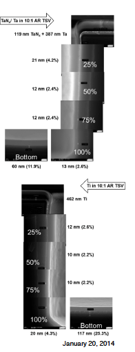
Weichart explained conventional vs. newer approaches, and the motivation for research to metallize 10:1 and higher aspect ratio vias. Directional PVD is still being used for via middle TSVs process flows, and cost is the biggest obstacle. So-called “long throw” low-pressure deposition takes place in continuous sputter mode, which requires a high amount of target material resulting in high cost per wafer, and doesn’t achieve the coverage percentages needed for HAR (Figure 1). Conformal coating on the sidewalls can’t be achieved, and too much material ends up in the bottom of the via. Oerlikon chose to use a high ionization density approach in a standard DC sputtering chamber by adding a high power pulse power supply to generate the high level of ionization in front of the target. They call it HIS (highly ionized sputtering).
Using this method, Weichart says that ionization close to the target is 90%. “By ionizing metal perpendicular to the substrate, we can reach the bottom of the via with sufficient coverage, as well as meet the coverage requirements on the side wall.” he noted. Weichart showed examples of different aspect ratio vias (Figure 2).
An additional tool feature for maintaining good morphology on the sidewalls is arctic chuck cooling. It also allows for higher deposition rates to be used on temperature sensitive materials, as deposition rates vary based on aspect ratios. Without arctic cooling, those rates have been constrained by the allowable thermal budget of the substrate.
The important message is that all this – regardless of the size of the vias, can be done on the same tool. “This is important to our customers with installed tools,” explained Koller. “We offer to upgrade our installed base to run TSV processes.” In addition to running standard UBM processes, customers will be able to upgrade existing systems to run HIS, and thereby widen the tools process versatility.
It is not, nor has it ever been Oerlikon’s desire to compete with the front-end PVD tool suppliers where they currently have no installed base. Rather, they are taking a pragmatic approach. Koller explained that for Oerlikon, the sweet spot for 2.5D and 3D ICs really lies in its established customer base: OSATs, packaging foundries, and pure-play foundries that are investing in middle-end and back end processes. The target applications therefore are via-last, and via-mid if the OSATS are handling the barrier/seed steps. There could also be promise in the interposer space. The CLUSTERLINE® tool is the one dedicated to 3D processes, noted Koller, as at this point, processes aren’t standard enough and volume isn’t high enough to warrant the use of the HEXAGON. However, the HEXAGON may come into play in its next generation, when 3D becomes more mainstream and processes become standardized, he said.
“For us, the question is more, where the 3D processes are done? If it’s in the front-end fab, we might not be a player. If it’s not in the front-end fab, then we will be a player,” said Koller. “We are watching the market closely to see where it’s headed. We have the technology available when it’s needed.” ~ F.v.T.


