
The Opportunities for RRAM Cells to Take 3D Stackable Memory to 8-nm Nodes
In Part One of this two-part series, we looked at the challenges that need to be overcome in manufacturing 3D stackable memory using the competing technology approaches. We will now focus on the advantages inherent in resistive memory technology over current NAND technology in taking 3D memory on a familiar and reasonable cost curve to 8-nm technology nodes. Let’s look at some of the attributes of resistive memory that can be used to address these factors.
Cell Functionality – RRAM in general has a lower off current, Ioff, than NAND, and as the cell scales, it requires only simple control circuitry. The RRAM cell is not electron based, and once the mechanism of filament formation is understood and able to be controlled, it has the ability to beat the performance metrics of NAND cells by an order of magnitude or more.
In order to be viable for stacking, the cell needs to exhibit two important characteristics. First, the cell should not add a significant thermal budget / stress from the process steps related to memory cell formation. The thermal budget should still be dominated by the standard back-end process used to deposit inter-metal dielectrics (ILD) and form the metal connections. Second, the memory cell should be able to withstand the thermal budget of additional metal lines that go on the top layers.
While creating something at a lower temperature that has the ability to withstand a much higher temperature may seem like a contradiction, it is a challenge that can be met by using select materials and material interfaces. Typically, material stability is proportional to deposition temperature, and so materials are expected to change as they go through a higher temperature process. If the resistive memory cell materials are targeted to specifications based on their post high temperature exposed state, there is a path for resistive memory cells to enable stacked 3D memory.
Today, resistive memory technologies are not being employed in many products, even for single layer memory. It is not that they lack adequate cell performance, but mainly because of manufacturing challenges. These challenges stem from many issues, including poor understanding of the risks involved with novel materials and the risk mitigation path for introducing new materials, new tooling required for depositing non-stoichiometric thin films, customized etch and cleans that require fabs to introduce new chemicals or slurries, etc. or interactions of new materials with existing CMOS processes. We will look at some of these factors and how to overcome them to successfully commercialize RRAM.
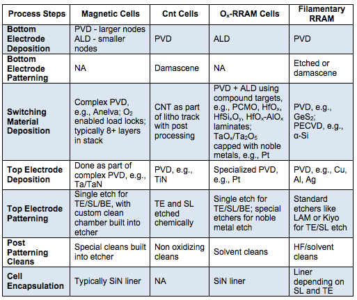
Process Tools – The obvious path to acceptance for RRAM cells is to find a way to make them using existing commercial equipment from the leading tool vendors. Having the starting point processes already developed on tools from multiple vendor also enables fast fab transfer and acceptance, because different fabs employ different toolsets for the same technology node. A typical list of process tools required for select novel memories is shown in Table 2.
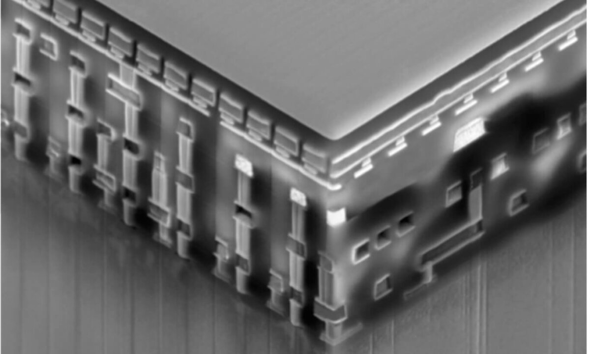
Process Steps – Most novel memories face the same challenge in early stages of development and foundry transfer – the stack etch. The more complex the materials in the stack, the more complex the stack etch, the tighter the mask thickness tolerances required to etch the materials in the stack and the more precise the tailoring of over-etch margins needs to be. These challenges are represented pictorially in Figure 2.
As shown in Figure 2, when etching complex stacks with multiple layers that are each only a few nanometers thick, the selectivity of the etch and post-etch cleans to different layers is challenging (1). This is typically resolved by having custom etchers with built-in clean chambers. The cell is protected from oxygen or fluorine from the inter-metal dielectric deposition process using a SiN spacer (2). The bottom electrode can be done as part of a via or as a damascened metal with its own mask (3). Etching complex oxide-based resistive memories leaves behind sidewall residues and requires custom cleans (4). Over-etch management is difficult when some of the etches are more physical in nature (i.e., ion bombardment) rather than chemically reactive (5). Breaking the stack into two masks, where the top electrode (TE) and switching layer (SL) edges are separated from the bottom electrode (BE), avoids sidewall leakage across the cell with no need for special cleans (6).
The key to the adoption of a new cell in volume foundries is to have a minimal number of layers in the switching material (and preferably a single material that requires no post-deposition treatment), conventional materials for the top and bottom electrodes and a post-etch clean that is already available in the fab. The simpler structures and materials lower the cost per bit. Using two masks to form the cell instead of one may seem counterintuitive, but while an extra mask adds to cost, it also removes the need for custom etchers and cleaning solutions and improves bit yield by avoiding sidewall leakage across the cell.
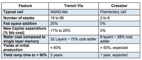
Yield – Conventional NAND cells are now being stacked in three dimensions to extend capacity scaling. Yields for stacked layers connected by through deep-trench vias are lower than for stacked layers that repeat the pattern. The pros and cons from a manufacturing standpoint for 3D NAND versus crossbar stack implementations are summarized in Table 3.

A scalable cell with better performance enables increased capacities with a reduced number of layers. The initial yield and ramp rate are expected to be higher for a crossbar architecture.
Die Size – The biggest impact on cost per bit is from the die size. A scalable cell with better performance reduces process cost but not die size. Die size for back-end integrated memory is dominated by two factors: metal line widths and pitch and the area of the control circuitry relative to the area of the memory array.
Metal line widths scale with technology nodes. Memory fabs are more comfortable than logic fabs when shrinking metal line widths and going to aggressive metal pitches, although they use the same tool set. By using a combination of a front end from a larger node (like 40 or 28nm) and a more aggressive scaling of metal lines in the memory array area only, a robust high-density chip can be made with little or no additional capital cost. No new lithography tools are required.
One of RRAM’s main advantages is using the area on the die more effectively by its ability to employ a single transistor to drive multiple resistive memory cells in an array. This is referred to as a 1TnR array or 1TnSnR array, where n is a number, T is the transistor, R is a resistive memory cell and S is a selector.
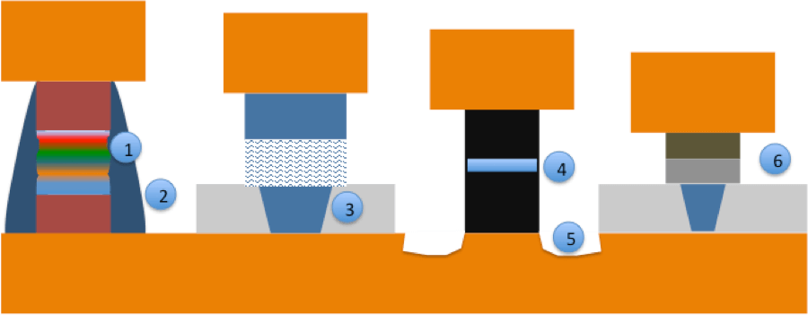
In some emerging memory technologies, the selector is implemented as a separate layer. In the example of the Crossbar RRAM cell, the selector is built into the cell itself. The greater the ability of the selector to select a particular cell and mute the other cells – reduce the sneak path current – the lower the circuit overhead and the better the performance from a cell crosstalk perspective. For the patented Crossbar FAST selector, n can be greater than 1000, which frees up a lot of area under the passive crossbar array to place peripheral circuits. This greatly reduces die size, as shown in the schematic in Figure 2.
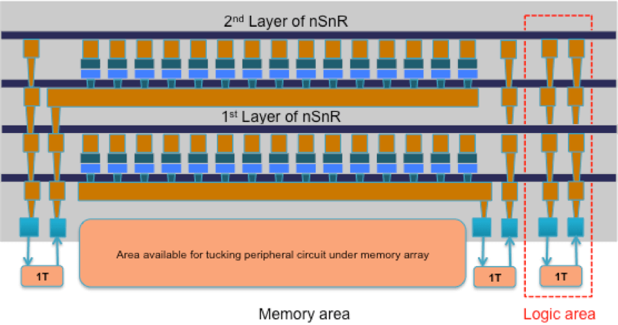
By using existing fab tools to create smaller line widths in the memory area on a 1TnSnR architecture with 1000+ cells driven by one access transistor, significant reductions in die size are possible.
Conclusion
Emerging novel memories that have cell characteristics superior to those of current NAND cells must overcome manufacturing challenges to become mainstream offerings. Most of these challenges are related to cell performance and cost per bit. By keeping the structure of the cell simple and by using a different approach to integration, these challenges can be overcome. ~ S. Narayanan


How does RRAM affect fit in with Intel/Micron 3D XPoint tech. Are they both marketable, or mutually exclusive?