
As traditional semiconductor scaling becomes increasingly complex and cost-prohibitive, transitioning from planar chip packaging architectures to 2.5D/3D stacked die package architectures has become key to enable the integration of greater amounts of chip functionality in smaller form factors. This need for form factor reduction, together with smaller process geometries and higher-count I/O on integrated circuits (ICs), is persistently driving adoption of advanced 3D wafer-level packaging (3D WLP) technologies and high-density interposer concepts. However, moving these stacked die packages into production reality creates new manufacturing and cost requirements that must be addressed across the wafer fabrication process.
Through-silicon-via (TSV) interconnections are key components for 3D device integration, since they enable electrical through-chip communication through stacks of vertically integrated layers on the wafer. TSVs promise tremendous advantages over traditional wiring such as: (1) improved electrical performance by reducing the interconnect length; (2) greater functionality through heterogeneous integration of chips (e.g. memory on logic, processors and sensors, etc.); and (3) increased integration density, which leads to smaller package sizes. As the industry ramps to high-volume manufacturing (HVM) on a variety of devices with these requirements, the wafer processing equipment used to manufacture these devices will require streamlined cost of ownership (CoO), translating into both enhanced throughput and innovative processing capabilities. This is particularly true for photoresist and lithography processing for mid-end-of-line (MEOL) processes.
MEOL technologies are found in the overlap area between different semiconductor business models and have become a strategic area for foundries, outsourced semiconductor assembly and test (OSAT) companies, wafer-level packaging houses and integrated device manufacturers (IDMs). Therefore, there is a strong interest from equipment suppliers to address the needs of the industry in the MEOL field. For 2.5/3D technology in particular, there is an increasing need to meet specifications from different process modules such as micro bumping and redistribution layers where pitches continue to shrink. This two-part article series will review several challenges associated with 2.5/3D integration and recent tool developments for MEOL processing that support 2.5/3D integration. Part one looks at ways to alleviate TSV stress.
TSV Interconnect Challenges
Despite the potential benefits associated with 3D and interposer-based 2.5D designs, the incorporation of TSVs poses significant challenges to the performance and reliability of 3D WLP. These include: containing electrical losses in TSVs due to insertion loss and crosstalk; and attaining lasting reliability of the TSV interconnects, which is caused by thermal induced stress resulting from the coefficient of thermal expansion (CTE) mismatch between the interconnect metal and the silicon substrate.
The formation of TSV interconnections requires a series of process steps, such as thinning and bonding the wafer/die to a carrier wafer prior to the formation of the vias. Each step acts as an additional source of stress that can affect the chip-stack performance. While wafer thinning is accompanied by a relaxation of pre-existing internal stress, the stress load generated by TSV fabrication adds additional stress to the global stress budget of a TSV stack (which typically includes package bumps, interconnects, thinned substrate with TSV, micro-bumps embedded in adhesive, a second layer of interconnects, transistor die, etc.) and can interfere with the adjacent features in the stack.
This stress can be sufficient to permanently degrade device performance, induce mechanical failure caused by cohesive cracking in the silicon, and cause delamination between the TSV and the silicon matrix. Ultimately, thermally induced stress can cause TSVs to pop-up from the silicon wafer and damage BEOL structures permanently. Accordingly, the incorporation of TSVs has to be carefully designed to inhibit parasitic effects on the 3D stack caused by thermo-mechanical reliability issues. This includes adding “keep-out zones” (KOZs) around every TSV where no devices should be placed in order to minimize the risk of stress affecting the electrical performance of transistors that are too close to the TSVs.

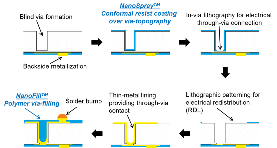
To alleviate these issues, the EVG®150XT resist coating and developing system with NanoSpray™ technology (see Figure 1) has been developed for applying photoresist and other functional polymers at and within TSV geometries to act as a stress buffer between the silicon and copper. Used in conjunction with the novel EVG®NanoFill™ process, this solution can create passivation layers that not only protect against corrosion, but also enable isolation to reduce electrical noise, as well as create compliant layers to mitigate thermal stress and permanent passivation of the interconnect.
The integration of EVG’s NanoSpray technology for conformal via lining and passivation with other complementary processes like the novel NanoFill technology for void-free via filling for permanent passivation and planarization, enables both high productivity and innovative approaches to resist processing for advanced WLP applications (Figure 2).
Use Case: Conformal Polymer Coating in TSVs
It is difficult to achieve a conformal polymer coating in deep cavities, along steep side walls and within the extreme aspect ratios of TSVs. This is mainly due to the fact that standard surface coating methods, such as spin coating and dry film lamination, were not developed to meet the requirements posed by today’s high aspect ratio microstructures. Therefore, new and innovative approaches are needed to meet these challenges.
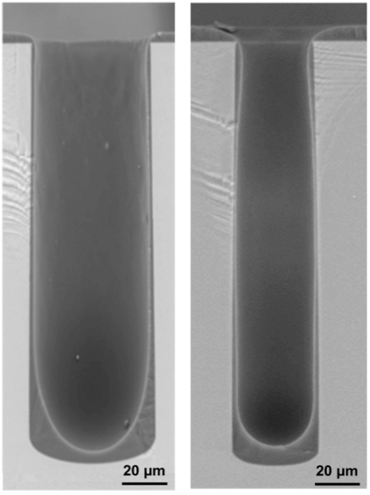
For tapered shallow vias, conventional spray coating is one of the most promising technologies to overcome current barriers. However, reflow of the resist after spraying can occur on the structure’s corners, which results in reduced edge coverage. Due to the flow behavior (viscosity and surface tension) of the resist materials, possibilities for optimizing the coating process are limited. Thus, coating vertical vias with conventional spray deposition technology can be challenging. Above a certain aspect ratio in combination with certain materials, it can even result in a lack or complete absence of sidewall coverage in the vias. In Figure 3, two SEM cross-sections are shown, depicting the conformal coating results of the NanoSpray coat process in 200µm deep vias with aspect ratios of 3.6 and 5, respectively.

Investigations on these polymer-lined TSVs have demonstrated electrical improvements, including a significant reduction in capacitance density compared to conventional SiO₂ insulating TSVs as well as an outstanding reduction in leakage current. The intrinsic mechanical properties of polymer-coated via sidewalls also allow for new TSV design solutions that are more forgiving on CTE mismatch-induced stress between the silicon substrate and the interfacing metal. Detailed investigations on the characteristics of thermal-stress-induced delamination for TSV structures have shown that long-term reliability can be significantly improved by reducing adverse impacts of thermal expansion mismatch.
About the Tools:
EVG150XT Automated Coating System
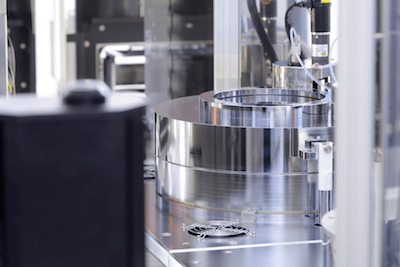
The EVG150 XT combines EV Group’s patented NanoSpray technology (Figure 4) with deep expertise in lithography-related processes on the XT Frame platform to enable the industry’s first HVM resist processing system for advanced wafer-level processing of a wide variety of mid-end and back-end interconnect applications. The EVG150 XT accommodates nine process modules, which enables high throughputs of up to 100/wph. These high throughputs can be achieved even for thick resist applications, such as those used in wafer bumping. Leveraging EVG’s XT Frame platform, the EVG150 XT embodies a modular and fully-automated HVM platform comprising a complete suite of tool modules for photoresist processing applications, including coaters, developers, metrology and photoresist strip. The tool supports wafers up to 300mm in diameter and is optimized for high throughput and maximum productivity. During in-line processing, high throughput is accomplished by operating up to nine individually combinable process stations in parallel mode, while wafer handling times are minimized by the high-speed linear transport system. Uptime has been further improved by increasing the reliability of each component and simplifying service and maintenance procedures.
EV Group’s NanoSpray technology can provide conformal coating of structures that have vertical sidewall angles—such as TSVs, through-glass vias and other through-substrate interconnects used for 2.5D interposers and 3D-ICs—with thick polymer liners and photoresists (from 1-10µm thick) cost-effectively. NanoSpray has already been adopted by multiple customers due to its ability to improve electrical performance characteristics, such as reducing insertion loss, crosstalk and leakage current, as well as reducing mechanical stress in TSVs. NanoSpray technology is available on EVG’s 200-mm resist processing platforms as well as its latest-generation 300-mm resist processing systems, such as the EVG150 XT, which provides up to a three-fold increase in throughput over prior-generation platforms.
In Part 2 of this article series, we will review a two-part case study on improving the thermo-mechanical reliability of TSV interconnects using EVG’s NanoSpray and NanoFill polymer-insulating TSV technologies.
About the Author
Dr. Antun Peić is business development manager at EV Group.
tel. +43-7712-5311-5341; E-Mail: a.peic@evgroup.com