


 I’ve been on a quest to find out more about EV Group’s new polymer filled TSVs since they first announced it in September. According to a company press release, NanoFill™ process is said to provide “void-free via filling of very deep trenches and high-aspect ratio (HAR) structures, and is suitable for all common polymeric dielectrics—offering a highly flexible, low-cost and production-ready via-fill platform for interposer development for 3D-integrated image sensors and other device types.” I caught up with Paul Lindner, EV Group’s executive technology director at the EV Group booth at IWLPC, and got some of the details.
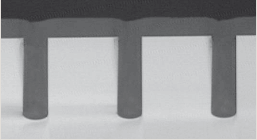
First of all, Lindner explained that this process targets larger via applications that use a via-last approach, where completely filling via with copper can add to the via stress due to the coefficient of thermal expansion (CTE) mismatch between Cu vias and the surrounding silicon. Think backside illuminated CMOS image sensors (BSI CIS), 2.5D Interposers, MEMS and LED applications. Unfortunately, replacing the copper with another conductive metal is not practical considering the ease of use and the established infrastructure. That’s why EVG came up with polymer filled TSVs. “Polymer replaces solid copper filling and helps with throughput and reliability,” he said. “When you’re working with larger dimension vias, there is a risk of stress near the via, and larger keep-out-zones are required.” In the case of EVG’s NanoFill process, the vias are lined with copper to form the interconnect, and then filled with the polymer. Lindner explained the process. After backside thinning and metallization, the via is formed and an in-via lithography step is used to open the bottom section of the via. Eletrodeposition (ECD) is used to put down a thin Cu seed layer. Next, using EVG’s proprietary NanoFill process, the via is filled with polymer and planarized. All together, Lindner says the processes take less time than filling with copper, which allows for improved throughput.
So why didn’t anyone think of this before? They did. Unfortunately existing spray and spin coating processes are limited for use with low-viscosity materials, and when attempted, there were issues with voids and trapped air. EVG has figured out ways to avoid this, and has developed a way to successfully achieve permanent passivation and planarization without forming voids or cavities using its EVG100 series of resist processing systems. Lindner says this process works with available dielectrics. “PCB is the favorite candidate, but it works with other spin-coatable products,” he said. Want to learn more? This recent technology feature in I-Micronews dives deeper into the details of polymer filled TSVs. (but still doesn’t give away the secret sauce. You’ll have to go directly to the source to get that.) ~ F.v.T.


