
Glass has many properties that make it an ideal substrate for interposers such as: ultra-high resistivity and low electrical loss, low dielectric constant, and adjustable coefficient of thermal expansion (CTE). Leveraging glass-forming processes such as Corning’s fusion forming process provides roughness < 0.5nm rms, and flat substrates with good stiffness. These properties provide opportunities for designers to use glass in new ways for improved packaging solutions.¹⁻⁴ In addition to enhanced technical performance, packaging solutions must also be cost effective. Glass substrates with through-glass-vias (TGV) provide a number of opportunities for improved performance and enhanced cost effectiveness. The fusion forming process gives the ability to form high quality substrates in large formats (>1m in size). In addition to scaling glass substrate size, it is possible to scale the process to deliver ultra-slim flexible glass to thicknesses down to ~100µm. Providing large substrates in wafer or panel format at 100µm thickness gives significant opportunities to reduce manufacturing costs.⁵⁻⁶
There has also been a lot of work in recent years demonstrating the ability to leverage and extend existing industry tool sets to fill glass vias with metal, apply surface redistribution layers, and demonstrate reliable structures.⁷⁻⁹ A sample of the latest advancements are provided below.
Glass Interposer Demonstrators
Figure 1 shows recent examples of both through (Figure 1a) and blind (Figure 1b) holes in glass substrates. Providing both through and blind holes allows the end user to leverage their existing equipment. For example, wafer based tools are best suited for filling blind vias and many panel-based approaches are suited for metallizing through vias.
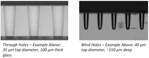
Figure 2 shows an example of using wafer-based tools at RTI International to fabricate Cu-filled, void-free blind vias. In this case, the vias had a 35µm top diameter and 125µm depth. They were metallized and background to 115µm thickness and single layer metal was provided on each surface to provide a daisy chain structure.⁷
A. Reliability Testing
We have previously reported the ability to maintain the high strength of glass substrates after hole fabrication.6 Of course it is also important to demonstrate good strength and reliability of filled vias and metallized structures.
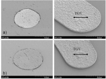
We recently reported results demonstrating excellent yield and 100 thermal cycle performance of fully filled blind vias after back grind and surface metallization fabricated in conjunction with RTI International.7 Reliability testing has continued and demonstrated the same performance after 500 cycles from -40°C to 125°C with 1 hour cycle time. The SEM images of the TGVs and routing metal before and after TCT are shown in Figure 3. This work is continuing to include 2-side metallization and performance after 1,000 cycles.
B. Glass Panel Fabrication
An important aspect of realizing cost effective glass interposers is to leverage the ability to manufacture in panel format and associated economies of scale. Many manufacturing tools exist today that enable fabrication of panel-based glass interposers and electronic components including steps for via fill and lithography.
One particularly attractive method to fill through holes in thin glass panels is to process them using a double side plating process as shown in Figure 4.
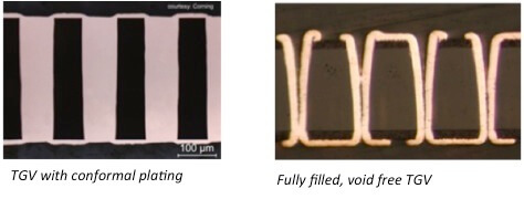
Figure 4 shows examples of metallizing TGVs with both conformal (left) and fully filled (right) plated glass via. On the left is a a daisy chain structure of conformally plated through vias processed at Georgia Tech’s Packaging Research Center (PRC).9 On the right is void-free fully filled through vias provided by Atotech.8 Atotech’s Semi-Additive Process (SAP) is an approach that should provide significant opportunities for enhanced throughput and cost-effectiveness. The choice of conformal vs. fully filled vias is dictated by application and integration strategies, for example.
There are challenges in applying standard plating processes to glass, but Atotech has recently reported significant progress in the ability to metallize glass vias using new adhesion promoters.8 The advantage of this approach is that it has the opportunity to leverage existing plating tools and techniques in the industry and provide excellent throughput.
Panel Level Lithography
Once the holes are filled, it is necessary to have panel-level tools to achieve electrical redistribution with fine line and spacing. The thermal stability and low roughness of glass relative to organic substrates provides the opportunity to approach line/space that is achievable in silicon, but in a panel format. Couple this with advancements in the ability to fill holes in a thin glass panel format, significant cost advantages will be realized without compromising L/S requirements. There is an opportunity to leverage tools designed for the flat panel display (FPD) industry to achieve < 3 µm L/S.7

Recent work has been done with Rudolph Technologies’ Jetstep S3500 substrate tool, which clearly demonstrates the ability to use advanced packaging toolsets to fabricate fine line and spacing structures on a 370x470x0.3mm glass panel. A team comprising Corning Incorporated, i3 Electronics, Rudolph Technologies, and Frontier Industrial Technology worked together to demonstrate ability to apply a single layer Cu metallization to ~3.0µm L/S. A Cr adhesion layer (50Å thick) followed by a Cu seed layer (2500 Å thick) was sputter deposited to provide the communing layer for subsequent SAP processing. A photoresist layer ~4µm thick was applied and exposed/developed into several evaluation patterns such as polar/star, escape, and interdigitated structures for continuity and bias/leakage testing) targeting 1-10µm L/S structures. The panels were then plated, stripped, and etched. Figure 5 shows the example of the metal structures across the panel.
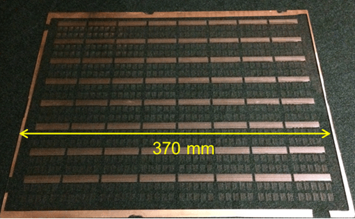
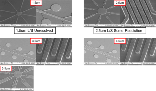
Figure 6 shows a close-up view of resolution achieved in 1.5 – 5.5µm structures. The process was able to fully resolve features 3.5µm and greater. Features 2.5µm in size were partially resolved. Features 1.5µm in size were not fully resolved but this is believed to be due primarily to non-optimal photoresist thickness and lithography settings. It is fully expected that additional work would enable the ability to resolve features < 3µm in size.
Conclusions
The electrical performance of glass; tunability of material properties such as CTE; and ability to form in thin, large sheets of high quality generates tremendous incentive for using glass as a TGV substrate for 2.5D and 3D applications.
The ability to generate well-formed through and blind vias has been demonstrated, and fully populated test vehicles using glass interposers have been created. This work shows that existing metallization technology can be leveraged to generate very good Cu filling performance in glass in both wafer and panel formats.
As reported here, significant process learning and development has been realized in wafer formats with very good results. Test vehicles indicate that good electrical, thermal, and reliability performance can be achieved using glass vias and the expected advantages in electrical performance of glass relative to silicon have been demonstrated in previous work.
We report here initial progress in the ability to fabricate and handle large and thin glass panels. With glass, opportunities for truly cost-effective interposer solutions with improved reliability exist, and sustained demonstration of downstream processing continues to move these solutions closer to commercialization.
Authors
Aric Shorey and Scott Pollard,Corning Incorporated
Philippe Cochet and Klaus Ruhmer, Rudolph Technologies
Alan Huffman and Matt Leuck, RTI International
Acknowledgments
We acknowledge the strong support from Atotech, Frontier Technologies, i3 Electronics, ITRI and Georgia Tech’s Packaging Research Center for this work.
References
- Kim, J, Shenoy, R., Lai, K-Y, Kim, J., “High-Q 3D RF Solenoid Inductors in Glass”, Radio Frequency Integrated Circuits Symposium, IEEE 2014.
- Shenoy, R., Lai, K-Y, and Gusev, E., “2.5D Advanced System-in-Package: Processes, Materials and Integration Aspects”, ECS Transactions, 61 (3) 183-190 (2014).
- Lai, WC et al., “300 mm Size Ultra-thin Glass Interposer Technology and High-Q Embedded Helical Inductor (EHI) for Mobile Application”, International Electronic Devices Meeting (IEDM),(2013).
- Qin, X, Kumbhat, N., Sundaram, V., and Tummala, R., “Highly-Reliable Silicon and Glass Interposers-to-Printed Wiring Board SMT Interconnctions: Modeling, Design, Fabrication and Reliability”, Electronics Components and Testing (ECTC), IEEE 62nd (2012).
- Shorey, A; Pollard, S.; Streltsov, A.; Piech, G.; Wagner, R., Electronic Components and Technology Conference (ECTC), IEEE 62nd (2012).
- Keech, J.; Piech, G.; Pollard, S.; Shorey, A., “Development and Demonstration of 3D-IC Glass Interposers”, Electronic Components and Technology Conference (ECTC), IEEE 63rd (2013).
- Shorey, A et al, “Advancements in Fabrication of Glass Interposers”, Electronic Components and Technology Conference (ECTC), IEEE 64th (2014).
- Fu et al., “Adhesive Enabling Technology for Directly Plating Copper onto Glass/Ceramic Substrates”, Electronic Components and Technology Conference (ECTC), IEEE 64th (2014).
- Demir et al., “First Demonstration of Reliable Copper-plated 30 µm Diameter Through-Package-Vias in Ultra-thin Bare Glass Interposers”, Electronic Components and Technology Conference (ECTC), IEEE 64th (2014).