

While most of the research institutes in the US and Asia have been focused on commercializing 3D integration technologies for mass markets such as mobile devices and consumer electronics, one US-based research institute has followed a different path more similar to that of the European research centers; focusing its 3D efforts beyond the mainstream to develop technologies for specialty applications in defense & security, high performance computing, medical electronics, and other areas. At this year’s ECTC 2014, May 27-30, 2014 in Orlando, I sat down with Dean Malta, technical manager, 3D Integration and Advanced Packaging, to learn more about Research Triangle Institute (RTI) International, located in Research Triangle Park, NC, and its involvement in 3D technology development.
According to Malta, RTI has a long history in the development of electronic technologies, including MEMS, advanced packaging, and 3D integration. “The role of our organization is somewhat unique in the field,” he explained, “As a research and development institute, we strive to contribute to the overall advancement of the technology, while acting as a development foundry and partner for a variety of government, commercial, and academic clients. As an independent, nonprofit organization, we provide open access to our technologies, including support for clients with custom and low-volume applications. This model is well suited to supporting customers who are doing advanced application and new product development for defense and aerospace systems, among others.”
RTI’s cleanroom facility includes a range of fabrication and wafer-level packaging capabilities, complimented by onsite testing and analyticallab facilities. Development and foundry services span a number of areas of advanced electronic packaging and integration. There are no front-end IC fabrication activities at RTI, however RTI does process customer-supplied IC wafers for 3D and wafer-level packaging purposes. “We offer a variety of services for advanced technology development, prototyping, and low-volume production, including custom or application-specific process flows,” said Malta.
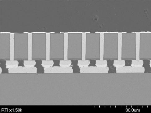
Specific to 3D, activities include custom via-last process flows, wafer-level bumping, RDL metallization, wafer thinning/handling, and assembly of 3D stacks. They can also accommodate a via-middle (MEOL) process flow starting from the point of receiving full thickness TSV-middle IC wafers, much like the commercial OSAT companies would offer (Figure 1). On the wafer-level-packaging (WLP) side, capabilities include solder bumping and wafer-level chip scale package (WLCSP) flip chip and multi-chip module (MCM) assembly, high-density micro-bump interconnects, MEMS wafer level vacuum packaging, and characterization of emerging electronic materials.
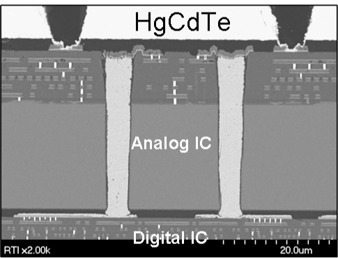
Malta said they’ve been developing a variety of TSV and 3D integration process flows for 3D IC stacking and Si interposers, and have been involved in the development of a number of interconnect bonding methods, such as Cu-Cu bonding at 5-10µm pitch.
One of RTI’s specialties has been high density TSVs and interconnect bonding driven by focal plane array image sensors that require tight pitch TSV and micro-bump arrays (Figure 1). They’ve also been working on silicon interposers for various applications and recently partnered with Corning Glass to develop via filling and overburden removal for glass interposers.
Overall, RTI’s focus is on the development of platform process capabilities or modules for advanced integration and packaging approaches. These modules can then be implemented in a variety of applications, for example medical imaging, aerospace and defense, flexible electronics, MEMS, and wearable systems. In theory, lower density requirements, such as 3D packaging, can be accomplished because high-density integration capabilities have been achieved.

“We want to develop processes that are transferable to volume production, but we are not focused on being the ultimate foundry supplier for high volume applications.” Malta explained. “RTI’s goal is to help advance the technology,applying it for development purposes and to specialized application areas.”
But 3D is not the only thing that’s happening at RTI. “We’re particularly interested in RF and heterogeneous integration, imaging technology, MEMS sensors, vacuum packaging, and flexible electronics technologies,” noted Malta “These things start out as separate development activities, but at any moment a few of them can come together in a given application.”
RTI’s approach to 3D is yet another example of how 3D integration doesn’t need to be mainstream to be a reality. ~ F.v.T


