


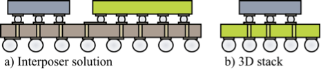
Currently in advanced integration, mainly stacked solutions (Figure 1b) are considered due to their attractive compactness. But if the ASIC or the processor is a high-performance circuit, there are problems with the thermal budget of the stacked solution. This is because the valid temperature range of the memory is limited. Designing a thermally balanced solution is very challenging and often ends up in expensive cooling concepts. Furthermore, 3D stacking requires “active” TSVs within the processor, which still is cutting edge technology and closely related to higher yield losses compared to package-based stacking solutions.
Interposer-based memory processor integration solutions (Figure 1a), on the other hand, represent a good alternative, relaxing the aforementioned challenges. The interconnect density requirements for high-pin-count components (e.g., Wide I/O) can’t be met by PCBs with their compound materials (even HDI) due to the limited line/space and via diameters.
Interposer Technologies
Interposer implementations consist of different technologies (e.g. front-to-back contacts (TSVs), interconnects, pads) for which independent solutions were developed during the last few years. But the independence brings along some questions: Can these different solutions be integrated considering technological aspects? And if there is a viable technological combination, does it make sense in electrical and economical perspectives?
If we look to the 3D world, currently different TSV technologies with different filling materials, different diameters, and as a result different thicknesses are in the portfolio. Looking to interposers, additionally also different interconnect technologies with different widths, pitches, and electrical characteristics are available. Interposer interconnects can be manufactured with different schemes, e.g. with planarized or non-planarized materials. The resulting surface topology limits the maximum number of interconnect layers.
Considered Systems
In the following, we will focus on high-performance applications, especially the side-by-side integration of a processor and a memory (e.g. Hybrid Memory Cube (HMC), (High Bandwidth Memory (HBM ), and Wide I/O and the processor or ASIC as illustrated in Figure 1a). The chips are mounted onto the interposer with micro balls or stud-bumps. The stud-bumps are made of Cu with 20µm diameter, 40µm standoff, and 40×40µm pitch as specified in JESD229. The interposer is molded and assembled onto a PCB board with 200µm diameter balls (Table 1).
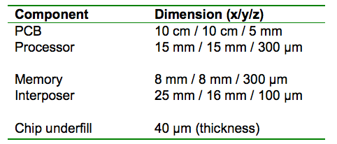
The size of the memory die itself is at least 8 by 8mm² and the pads are placed on all sides. The routing of the longest interconnects from the pads of the memory (on the opposite side) to the border of the memory is 8mm. With a given determined maximum interconnect length of 20mm (for Wide I/O memory) only 12mm are available for the routing between the chips.
Different TSV technologies
Currently, different TSV diameters are available or under discussion. If we assume that for handling a minimum interposer thickness of 100µm and a manufacturable aspect ratio of 1:10 is given, the resulting upper limit for the TSV diameter is 10µm. The biggest possible TSV diameters are in the range of 300µm. TSVs with a diameter bigger than 70 µm are typically hollow (i.e., not completely filled with a conductive material) due to better mechanical stress characteristics. But lower resistance TSVs are necessary for power ground routing; alternatively multiple TSVs must be used in parallel. In high performance applications with signal routing on both sides of the interposer the TSV diameters range between 10 and 40µm.
Different dielectrics, number of layers, and line spaces for the metal layer
As mentioned above, for silicon interposers basically two different options for the dielectric material exist; namely SiO₂ and polymers. SiO₂ can and must be planarized by chemical mechanical polishing (CMP), which is not possible with polymers. On non-planarized surfaces, the achievable resolution of line/space features is lower compared to flattened surfaces. This is because advanced lithography faces severe limitations on flat surfaces. On the other hand, every CMP step increases the overall costs.
The manufacturing processes for SiO₂ based stacks are derived from the (upper layer) metallization processes in classical 65nm or 45nm technology nodes. Typically, up to five layers are fabricated for such stacks. The resulting minimum line/space is in the range of 100 to 500nm. These metallization technologies are usually combined with TSVs with a diameter of 10µm. The majority of the SiO₂ based interposers directly expose the TSVs on the backside to mechanical and chemical-mechanical processes combined with the deposition of one additional metallization layers for the pads.

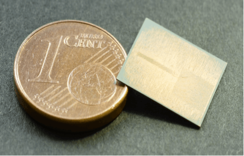
On the other side, we have polymer based stacks with 2 or 3 metal layers on top as well as 2 or 3 metal layers on the bottom side. In this approach, the TSV diameters are also 10µm, but the metal line/space is in the range of 8µm to 10µm. This option is especially interesting for low-cost interposers because most of the CMP process steps are omitted and also the masks for the lithography are cheaper due to lower resolution requirements. Figure 2 shows an interposer designed and fabricated at Fraunhofer. It is a silicon interposer with a polymer material used as dielectric for the metallization (parameter values close to polymer 1 in Table 2).
Electrical impact
If SiO₂ based stacks are applied, smaller line/spaces are possible in comparison to the polymer approach, while the TSV diameters are comparable. As a result we have the same parasitics for the TSVs in both cases.

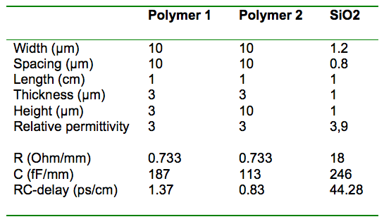
But on the other side, the parasitics for the interconnect structures differ a lot (see Figure 3 and Table 2). The smaller interconnects of SiO₂ stacks should results in smaller capacitances because the area for coupling is much smaller. The relative permittivity of SiO₂ is 3.9 and 3-4 for polymers. Hence, assuming identical dielectric thickness the influence on parasitic capacities is comparable.
Then again, the polymer approach offers a higher flexibility with regard to the polymer thicknesses. Polymers can be deposited in fine graded steps with a high thickness (e.g., 10µm dielectric height, Table 2, Polymer 2). These thick layers result in reduced parasitic capacitances compared with SiO₂-based stacks (54% reduction in our examples). Furthermore, the interconnect resistance of polymer based stacks is smaller because of the larger interconnects. The cross section area of interconnect structures on polymer technology is 25 times larger compared with the SiO₂ technology. As a result it can be shown that the RC delay as a first order approximation for the interconnect delay can be better controlled on interposers with polymer stacks. If the polymers are thick enough, the RC delay of polymer stacks is 30-50 times smaller compared to SiO2 stacks (see Table 2).
Implication for the routing
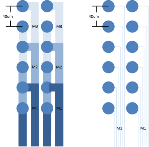
Summarizing the previous facts, the realization of interposer interconnects with a length of up to 2cm becomes a very hard challenge. Compared to chip layouts, we do not have the possibility to place buffers to drive long wires. The technological considerations also imply impacts on the physical design of the interposer. Figure 4 illustrates the impact of the technology decision (i.e., polymer-based vs. SiO2-based interposer) on the conditions for interconnect routing.
The increased width and spacing of interconnect structures on polymer-based interposers require a minimum of 3 metal layers for the break out routing of pads with a 40µm pitch (Figure 4, left). In comparison, for SiO₂-stacks only 1 metal layer is needed in the same example (Figure 4, right). This assertion is true for signal nets only. Power/Ground interconnects aren’t manufactured with the smallest possible line/space because the resulting resistance would be too high. Such high resistances imply problems with static and dynamic voltage drops and also with electromigration. In realistic scenarios at least 2 metal layers are required even for SiO₂ stacks. ~ A. Heinig


