

Last week, HotChips 2014 (aka HC26) was held at the Flint Center within the De Anza College in Cupertino, California. As in many previous years, I attended both the Sunday tutorial and the main conference on Monday and Tuesday. As usual, there were great keynotes and lots of interesting technology news.
The tutorial always focuses on an important technology or market trend. This year was no exception: Sunday morning Ruby Lee, a well-known security expert at Princeton, outlined a lot of basic terminology and operating principles in preparation for the afternoon presentations, focusing on the very hot topic: the Internet of Things (IoT). As I expect that IoT devices will be a high-volume opportunity for interposer-based designs, I followed attentively. I saw my expectations confirmed: IoT peripherals do need heterogeneous functions packed into a low-cost, low-power, and small form-factor IC.
Just like in previous years, high-performance and high-complexity chips were the main focus of the conference on Monday and Tuesday. But unlike before, ways to reduce power dissipation got a lot of attention in most presentations.
For me, the most interesting part of this year’s conference was clearly the SK Hynix presentation in the technology session on Monday afternoon. Joonyoung Kim showed how system requirements are projected to increase in regards to bandwidth, capacity, power efficiency, and form factor. He outlined why wire-bonding imposes big limitations on all four of these criteria and showed how TSVs contribute to meeting – or exceeding – these objectives in the first generation of HBM and far exceeding them in the second generation. See the slide below.
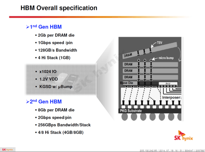
While I didn’t hear a release date for the 2nd generation HBM, I clearly heard that they have currently 21 ongoing design-ins. This high level of customer demand should encourage management to give HBM 1 and 2 their full attention.
The ThruChip presentation that followed also looked very interesting – but only at first sight. Dave Ditzel highlighted the drawbacks of wire bonding, and even attacked TSVs for being too costly. No doubt, he is correct that TSV processing can add $40-100 to the cost of a processed wafer. But his suggestion to use inductors for transmitting signals between vertically stacked die raised a number of concerns in my mind: ThruChip technology requires a coil diameter of three times the distance between wafers. With their only 4µm-thin wafers this means 12µm diameter or 113µm² of silicon area – if the coil is round. He actually showed square coils, which take 144µm² in area. Considering that IMEC and others have 2µm-diameter TSVs in development for 40µm-thick wafers, and Tezzaron is using 1µm-diameter TSVs for 10µm-thick wafers, I am not impressed by ThruChip’s inductive coupling area requirements.

Another question I have refers to inductive coupling between adjacent signals, to PLLs and supply lines. As DC power can’t be transmitted inductively, ThruChip suggests to use highly doped silicon vias for power and ground. Considering that these vias only need to be 4µm long, their voltage drop/power dissipation may be acceptable. I just wonder what kind of insulation they’ll need to the admittedly less but still conductive silicon substrate.
I really liked the third presentation in the Technology section a lot, because it showed the way silicon technology can enhance our lives in very creative and new ways. Arjang Hassibi showed biochips for low-cost, point-of-care molecular diagnostics that his company, InSilixa, Inc. in Sunnyvale, has developed. He showed that the current diagnostic and treatment options are time-consuming, costly, and not always fully effective, if the cause of an ailment can’t be identified correctly. Arjang explained how their current technology (Hydra-1K Biochip Module) works and how simple and compelling the concept of this cheap and very accurate DNA analysis device is and how widely it can be used.
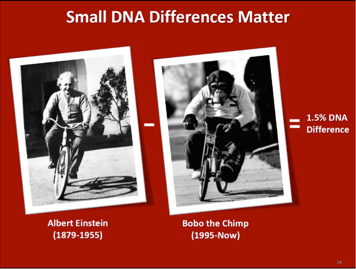
Last but not least, he demonstrated again his skills as cartoonist and showed his sense of humor: Did you know that there is only 1.5% difference between Albert Einstein’s DNA and the DNA of a monkey?
Full disclosure: I know the presenter from my Barcelona Design days (2000 & 2001), when I worked with his brother, also a very smart Stanford Ph.D. I hope that InSilixa can become a major player in the IoT space, make our healthcare system more affordable and shorten the time to diagnose and treat ailments. ~ Herb


Herb,
Good summary and write up.
Did you have to include the last picture of two bicyclists?
This might cause more thought/concern about the Planet of the Ape movies.
I will have to start sleeping with a nightlight on.
Bill
Herb :
Given their inherently higher bandwidth, they could get away for a while by multiplexing all the I/Os and still fit all those large coils needed for dice that have not been thinned down below current 50 um, w/o too much xtra real estate. Look up the original work that’s been going on in Japan for 5+ years..
Dev, thanks for followings my blogs regularly!
Could you share a pointer to the Japanese groundwork for this technology with me. At this time I am concerned – and admittedly TSV-biased – but clearly open to learn about inductive coupling.
Can I get a copy of the paper by Arjang Hassibi? Bill Moffat