
In order to remain competitive in the Internet-of-Things (IoT) environment, medium-sized industrial and process measurement technology companies must increasingly integrate their sensor circuits on ASICs (Application Specific Integrated Circuits). The semiconductor industry is currently meeting this need with lower costs for development processes and lower thresholds in terms of production quantities. However, this trend does not take place sufficiently in chip packaging. As a result, ASICs that require individual packages run the risk of failing the quantity hurdles of the package service providers that predominantly based in Asia. A Germany based consortium of seven partners from industry and research is now offering an alternative solution.
A good example of the above-mentioned requirement profile is a research project for radar sensors for industrial and process measurement technology, funded in part by the German Ministry of Education and Research (BMBF). The project is titled “Glass interposer technology for highly compact electronic systems for high-frequency applications” (GlaRA). The frequencies above 100 GHz, which are higher than that of cellular technology, and much stricter environmental requirements do not allow for the use of standard IC packages. These components have to be adaptable to specialized sensor ASICs and at the same time be able to be manufactured in medium quantities at competitive costs.
The consortium has set up and characterized a reliable interposer technology based on glass for broadband millimeter-wave modules with application in sensor technology and communication at frequencies above 100 GHz as a system-in-package (SiP). The modular technology system demonstrated represents a revolution for sensor packaging: Compared to the state of the art, it increases the functionality that can be integrated through various waveguide concepts, high-density micro-wiring and hermetic encapsulation. In addition, it enables applications up to 300 GHz thanks to its high levels of accuracy and material quality. This is achieved with glass a single system material, which allows among other things, excellent waveguiding properties and high-precision micro-machining.
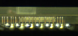
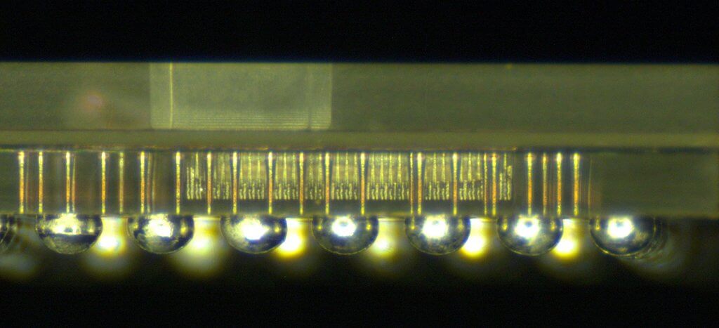
By using glass interposers with electrical feed-throughs (vias), a hermetic packaging was demonstrated in which the components are enclosed between two glass interposers (Figure 1). The packages are manufactured at the wafer level up to 300 mm in diameter. Wafer-level packaging is characterized by moderate costs due to the parallel processing of many components and an alignment accuracy within the tight tolerances of RF technology. For this purpose, adapted standard systems for the processing of silicon wafers are used, which greatly accelerates commercial implementation. Glass is also available in large panel formats, which makes scaling the manufacturing process up to large quantities much easier.
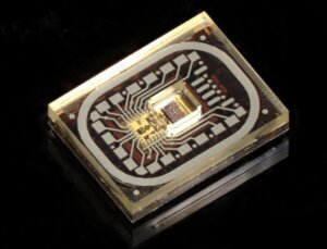
The results represent an extraordinary success for an R&D project funded by the BMBF. The consortium demonstrates this using an extremely compact radar front-end for future radar level sensors at an operating frequency of 160 GHz, which was set up at Endress + Hauser AG. The glass package measures tiny (5.9 mm x 4.4 mm x 0.8 mm) and contains a radar ASIC in SiGe technology, all electrical connections for connection to external electronics, test structures for characterization, and a waveguide connection, which can also be used as an integrated primary radiator for a lens antenna (Figure 2). Such future fluid level sensors are characterized by high distance resolution, measuring accuracy, and beam focusing combined with very compact dimensions. They are therefore extremely interesting for the ever smaller and more modular systems of smart process measurement technology.
The demonstrators were implemented using a novel process chain that begins with the revolutionary laser-induced deep etching (LIDE) from LPKF Laser & Electronics AG. The process for creating microstructures in glass completely avoids any damage to the glass substrate, which is what makes a manageable and hermetic glass package possible. The Fraunhofer Institute for Reliability and Micro-Integration (IZM) has implemented an industrial process for metalizing the through glass vias with high aspect ratios. In a wafer bonding process, the assembled components are hermetically packaged by joining two glass wafers, each of which has vias and cavities.
The structuring and metallization of the conductor tracks on the glass substrates are done by PacTech GmbH. The placement of solder deposits on the contact surfaces generated without external current is done by means of PacTech’s SB² process, a laser-based process for the sequential application of solder balls. Different alloys are used to enable a staggered assembly at different temperatures. MSG Lithoglas GmbH supports the implementation of the high-frequency packages by producing cavities that are used, for example, to accommodate the ASICs. High-precision spacers made of glass are also produced by means of a low-temperature coating.

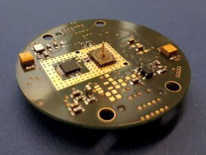
With a high-frequency concept for the new package developed by the Institute for Microwave Technology at the University of Ulm, the radar signal at over 100 GHz can both directly illuminate a lens via a primary radiator and also be routed to a remote antenna with little loss via a flexible dielectric waveguide (Figure 3). With the various options for emitting the radar signals from the package, a wide range of applications can be served. Sentronics Metrology GmbH has developed a 3D high-speed sensor with layer resolutions in the sub-nanometer range for quality control. The sensor has been qualified, among other things, for leak testing of encapsulated, evacuated glass packages.
The industrial partners are very interested in the future commercial availability of the technology. They see the potential for many other areas of application such as pressure measurement technology, liquid analysis, photonics, MEMS, medical technology, and communication technology beyond 5G.
The project “GlaRA” is funded from August 2017 to March 2021 under the reference 16ES0687K by the BMBF as part of the TechSys call for proposals.


